Manufacture of probe unit having lead probes extending beyond edge of substrate

Inactive Publication Date: 2005-09-20
YAMAICHI ELECTRONICS
View PDF7 Cites 37 Cited by
  • Summary
  • Abstract
  • Description
  • Claims
  • Application Information

AI Technical Summary

Benefits of technology

[0014]It is an object of the present invention to provide a method of manufacturing a probe unit having elastic beams extending beyond the edge of a substrate

Problems solved by technology

A probe unit to be used with such electrodes is difficult to be formed with a punching machine.
However, there remains some problem that some tight contactness is required between a plated underlayer and the substrate in the elastic lead region when the plated underlayer is formed and when the plated layer is grown and that some peeling property is required when the substrate is removed from the leads.
The shape of a fine probe may be deformed or damaged.
If the single substrate is used and this substrate cannot

Method used


Image

  • Manufacture of probe unit having lead probes extending beyond edge of substrate
  • Manufacture of probe unit having lead probes extending beyond edge of substrate
  • Manufacture of probe unit having lead probes extending beyond edge of substrate

Examples


example 1

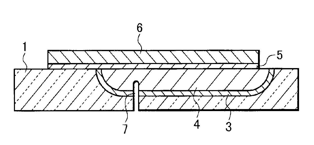
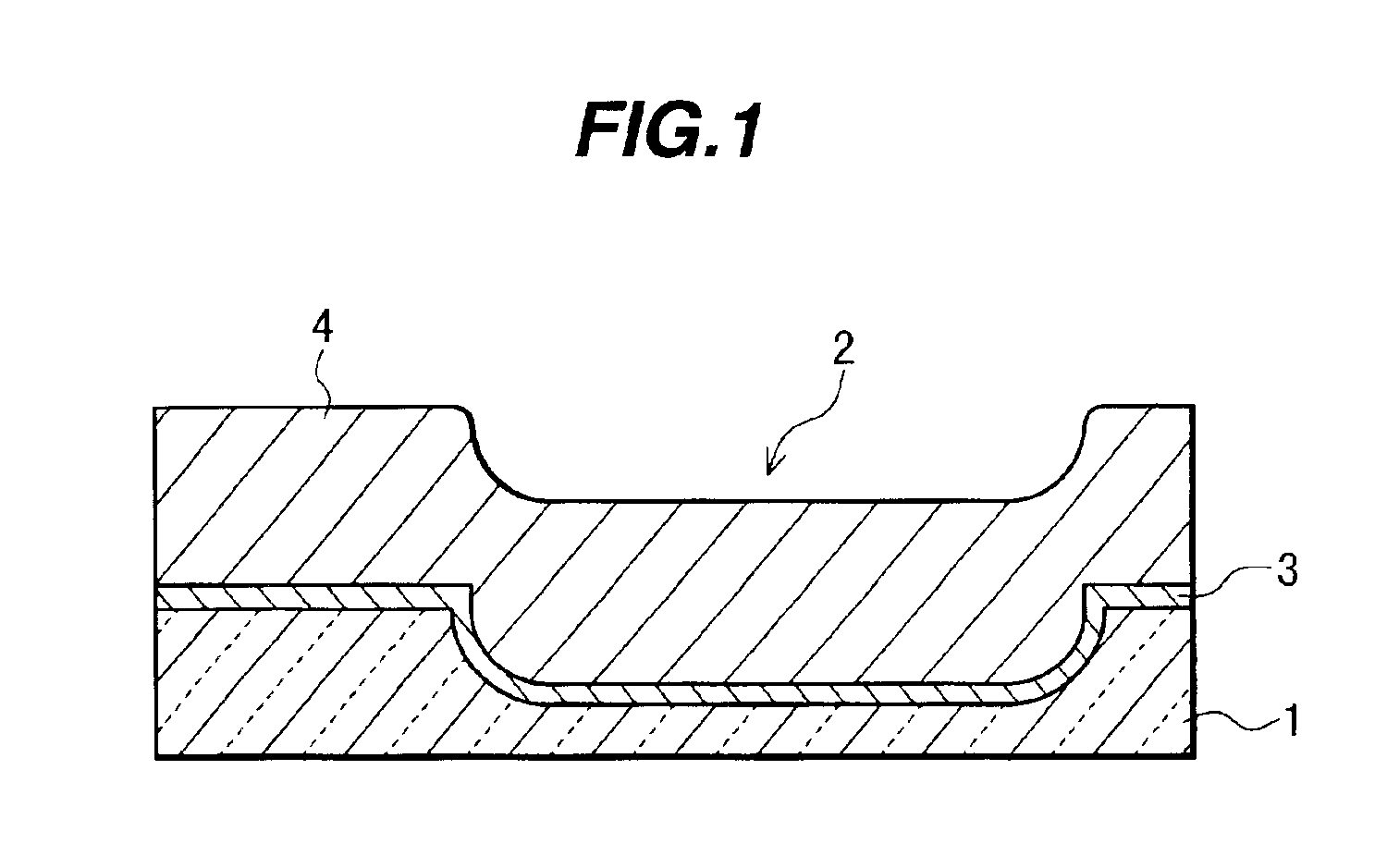
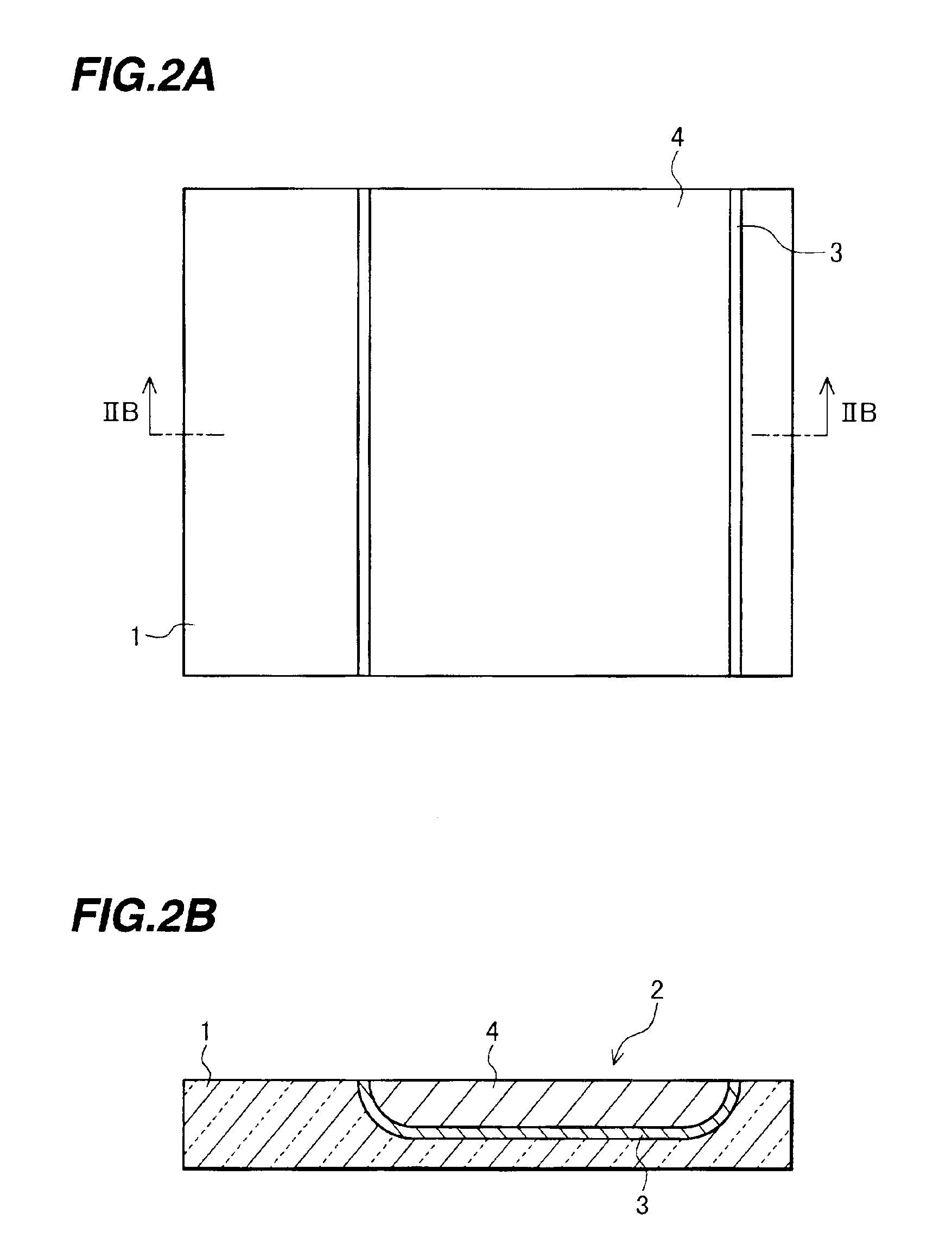
[0064]In one surface layer of a glass substrate of 76.2 mm square and 0.66 mm in thickness, a recess having a width of 5 mm, a length of 76.2 mm and a depth of 0.3 mm was formed in parallel to one side of the substrate. The cross sectional shape of the recess at opposing end portions had a smooth arc shape having a radius of 0.5 mm. Chromium as a tight contact layer was sputtered on the surface of the substrate on the recess side, and copper as a plating underlayer was sputtered on the tight contact layer. Copper was plated to a thickness of about 0.35 mm.

[0065]The substrate was roughly polished by using abrasive grains having a diameter of 3 μm and 1 μm, and then finely polished by using abrasive grains having a diameter of 0.5 μm. The substrate was planarized by removing the metal layer on the substrate excepting the metal layer in the recess. Voids did not exist in the plated copper in the recess.

[0066]On the whole surface of the planarized substrate, a probe plating underlayer o...

example 2

[0087]Through holes of 5 mm×10 mm were formed through ceramic substrates not baked each having a thickness of 100 μm by using a punching machine. Twelve ceramic substrates were laminated. The through hole of the ceramic lamination substrate was filled with conductive copper paste (product name: CF-2800 manufactured by Harima Chemicals Inc.). This copper paste contains 20 vol % solvent. Since the copper paste contracts when it is heated, excessive copper paste was filled in the through hole to such an extent that the copper paste is swelled over the through hole. The substrate was placed in an oven and heated to evaporate the solvent. The copper was completely filled in the through hole. The top and bottom surfaces of the substrate were polished. The metal layer was completely filled in the through hole, and overflowed metal in the area outside the through hole was removed to expose the ceramic substrate.

[0088]Leads extending above the through hole were formed on the substrate in the...

example 3

[0099]Photosensitive etching glass was used as a substrate. By shielding one end area of the substrate, ultraviolet rays were applied to the other area by using an exposure machine with a ultra high pressure mercury lamp as a light source. Here the ultraviolet rays may include G line (436 nm), I line (365 nm), and / or H line (405 nm). Ti and then Ni were sputtered to the whole surface of the substrate to form a probe plating underlayer.

[0100]Resist was coated on the substrate, prebaked, exposed, hardened, developed and washed to form a resist mask having openings in areas corresponding to leads. On the plating underlayer exposed in the openings, an NiW layer was plated to a thickness of 30 μm. Next the resist was removed by ashing and the exposed probe plating underlayer was removed by milling.

[0101]The ultraviolet ray radiated area of the substrate was etched by 5-6% hydrofluoric acid, and washed by pure water. The substrate was baked to form crystallized glass. A probe unit having ...


PUM


Abstract

A sacrificial layer is formed in a recess of a substrate, and leads extending from the substrate into an area of the sacrificial layer are formed. A cut is formed from the bottom surface of the substrate, the cut extending from the bottom surface to the area of the sacrificial layer via the substrate, then the sacrificial layer is removed. A probe unit can be obtained having the leads whose front portions extend beyond the edge of the substrate. A through conductor may be formed in a through hole formed in a substrate. Leads may be formed on a photosensitive etching glass substrate to thereafter selectively etch the chemically cutting type glass.

Description

CROSS REFERENCE TO RELATED APPLICATION[0001]This application is based on and claims priority of Japanese patent application No. 2001-086267, filed on Mar. 23, 2001, the whole contents of which are incorporated herein by reference.BACKGROUND OF THE INVENTION[0002]A) Field of the Invention[0003]The present invention relates to a method of manufacturing a probe unit having leads disposed in parallel at a small pitch, each lead extending beyond the edge of a substrate to form an elastic beam. The probe unit is used, for example, for a conduction test of electrodes of a semiconductor integrated circuit, a liquid crystal panel or the like.[0004]B) Description of the Related Art[0005]A conduction test of a semiconductor integrated circuit, a liquid crystal panel or the like is performed in order to check whether the test sample operates normally satisfying the specification. This conduction test is performed, for example, by pressing the front end of a probe unit against electrodes dispose...

Claims


Application Information

Patent Timeline
IPC IPC(8): G01R1/067G01R3/00G01R1/073G01R31/26H01L21/66
CPCG01R3/00G01R1/06727G01R1/07342
Inventor HATTORI, ATSUOYOSHINO, TOSHITAKAHAMANO, TETSUTSUGUSUGIURA, MASAHIRO
Owner YAMAICHI ELECTRONICS
Why Eureka
Try Eureka