Semiconductor device and an optical device using the semiconductor device

a semiconductor and semiconductor technology, applied in the direction of semiconductor/solid-state device details, discharge tube luminescnet screens, discharge tubes/lamp details, etc., can solve the problems of heat release rate dropping as the package is downsized, large contracting of the insulated base material, and difficult to maintain uniform shapes of the base material, etc., to achieve excellent reliability, excellent optical properties, and great accuracy

Inactive Publication Date: 2005-10-11
NICHIA CORP
View PDF5 Cites 187 Cited by
  • Summary
  • Abstract
  • Description
  • Claims
  • Application Information

AI Technical Summary

Benefits of technology

[0007]The outer shape of the package comprises thin film electrodes on an insulated base material. The insulated base material greatly contracts under high temperature and it has been hard to maintain uniform shapes for the base material. Furthermore, since this type of package uses thin film electrodes, the heat release rate goes down as the package is downsized. Consequently, the package includes a molded body formed by resin injection molding to try to make the light emitting device thinner and smaller, and to improve the rate of heat released from the device. Such a package is made by injection molding so that the lead electrodes can be inserted in the package.

Problems solved by technology

The insulated base material greatly contracts under high temperature and it has been hard to maintain uniform shapes for the base material.
Furthermore, since this type of package uses thin film electrodes, the heat release rate goes down as the package is downsized.
However, when a package is formed by injection molding, a tolerance is created when bending (forming) and this results in difficulty in obtaining uniform shapes in quantity.

Method used


Image

  • Semiconductor device and an optical device using the semiconductor device
  • Semiconductor device and an optical device using the semiconductor device
  • Semiconductor device and an optical device using the semiconductor device

Examples


example 1

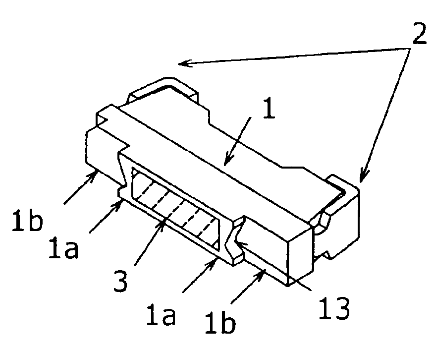
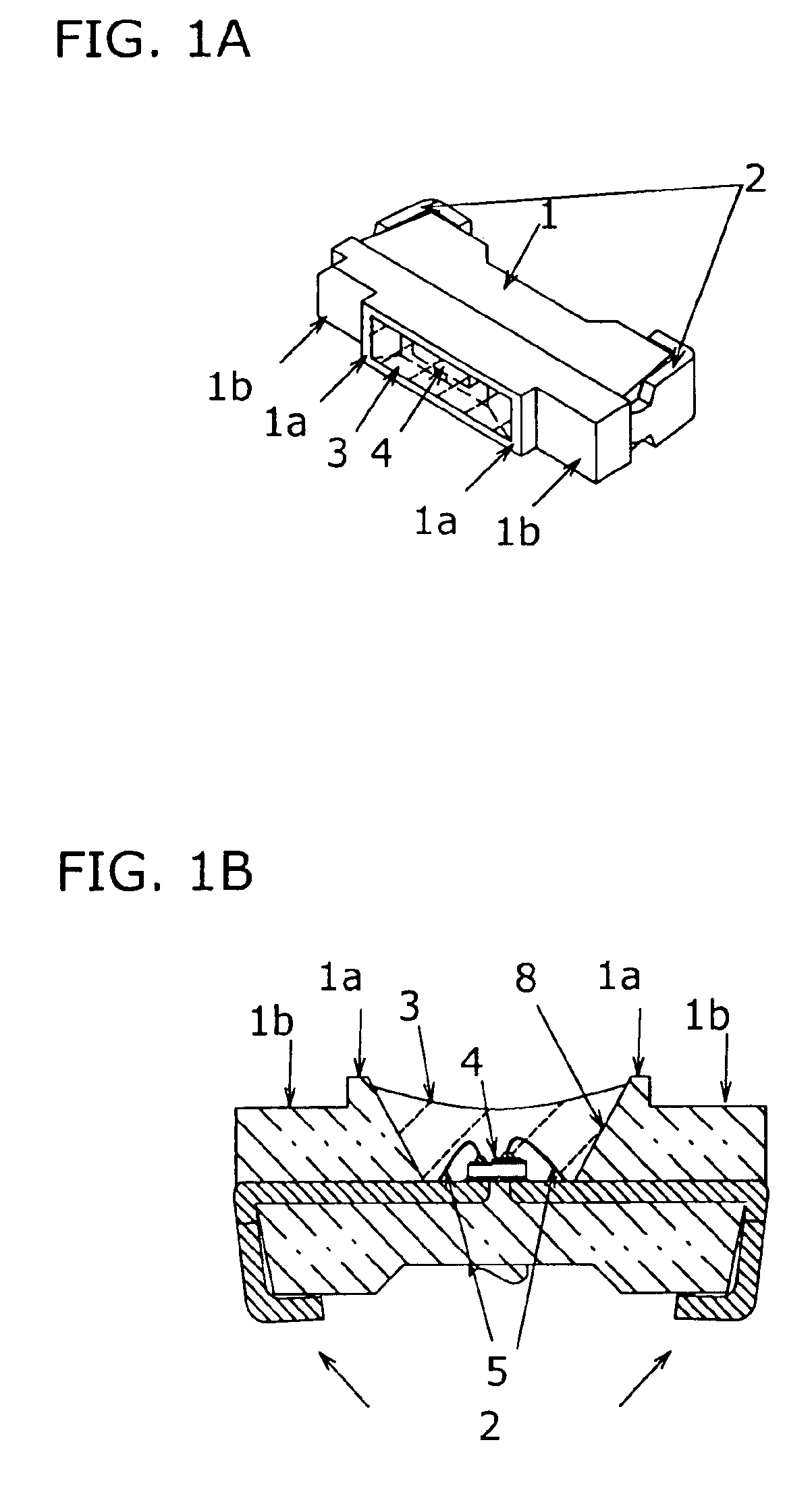
[0178]A surface mounting type of light emitting device is shown in FIGS. 1A and 1B. The light emitting element 4 is a nitride semiconductor element having an active layer of an In0.2Ga0.8N semiconductor with a monochromatic emission peak being a visible color of 475 nm. In more detail, the light emitting element 4 of the LED chip is made by flowing TMG (trimethyl gallium) gas, TMI (trimethyl indium) gas, nitrogen gas and a dopant gas together and forming a gallium nitride semiconductor layer in a MOCVD process. The layers of the N-type nitride semiconductor or the P-type semiconductor are formed by switching between SiH4 and Cp2Mg as the dopant gas.

[0179]FIG. 8 is a plan view of an LED chip of the present embodiment and FIG. 9 is a schematic cross sectional view of the LED chip taken along the broken line AA′ in FIG. 8.

[0180]The elemental structure of the LED chip of the present example is sequentially formed on a sapphire substrate 14. The layers include a GaN buffer layer of undop...

example 2

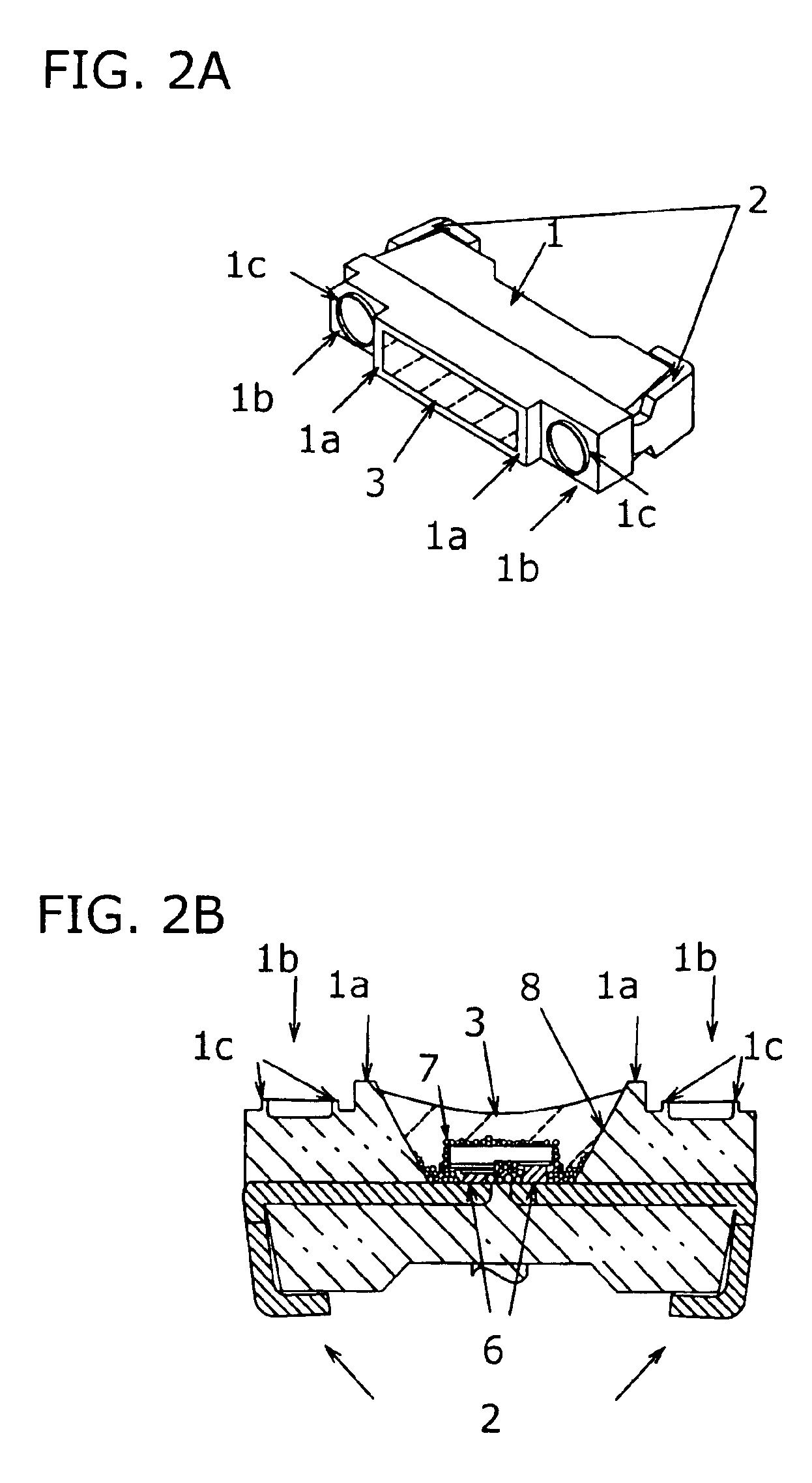
[0194]FIGS. 2A and 2B, FIGS. 3A and 3B, and FIGS. 4A and 4B show the light emitting devices in the present example. The light emitting devices are made in the same manner as in Example 1 except for having an outer circular wall 1c on the second main surface 1b of the package 1.

[0195]The light emitting device of the present example has an excellent reliability and a high quality attachment formed by bonding the LED to other members using an adhesive agent disposed inside the outer wall 1c while at the same time preventing the adhesive agent from flowing out past the outer wall into the recess.

example 3

[0196]FIGS. 2A and 2B, FIGS. 3A and 3B, and FIGS. 4A and 4B show the light emitting devices in the present example. The light emitting device is made in the same manner as the other examples of the present invention, except for forming a Au bump on the electrode of each LED chip, and employing a flip-chip method wherein ultrasound bonding is carried out so as to make the electric connection with each lead electrode that is exposed in the bottom of the recess of the package.

[0197]The light emitting device of the present example can achieve similar effects described in the above examples, and moreover, the heat releasing and light extracting properties can be enhanced.


PUM


Abstract

A semiconductor device comprising a semiconductor element and a support member having a recess for housing the semiconductor element is disclosed. The support member includes lead electrodes and a support part holding the lead electrodes so that a surface of tip portions of the lead electrodes are exposed in a bottom of the recess. A main surface of the support member has at least a first main surface disposed adjacent to the recess and a second main surface disposed adjacent to the first main surface. The second main surface preferably has a protrusion and a further recess. The protrusion preferably forms an outer wall around a depression. The semiconductor device having this configuration has excellent and accurate positioning and can be strongly bonded with other members. The semiconductor device can also be obtained with a high process yield.

Description

BACKGROUND OF THE INVENTION[0001]1. Field of the Invention[0002]The present invention relates to a light emitting device used in a back light of a liquid crystal display, a panel meter, an indicator light, a surface emitting optical switch, or the like. The present invention also relates to a light receiver device used in an optical receiver for an optical sensor, or the like, as well as the optical devices using the light emitting device or light receiving device.[0003]2. Discussion of the Related Art[0004]A semiconductor element can be used as a light emitting element or a light receiving element. Also, a semiconductor device can include a support part protecting the light emitting element and / or the light receiving element from the external environment, and lead electrodes connecting them.[0005]When used as a light emitting device, a light emitting diode is capable of emitting mixed light in a white range with a high intensity by a combination of light from a light emitting eleme...

Claims


Application Information

Patent Timeline
Patent Type & Authority Patents(United States)
IPC IPC(8): H01L33/00H01L33/20H01L33/48H01L33/58H01L33/62
CPCH01L31/0203H01L33/486H01L2224/49107H01L33/58H01L33/62H01L2224/32245H01L2224/48247H01L2224/73265H01L2924/1815Y10S362/80H01L33/20H01L2224/48091H01L2924/3025H01L2924/01322H01L2224/16245H01L2924/00H01L2924/00014H01L2224/05568H01L2224/05023H01L2224/05001H01L2224/05184H01L2224/06102H01L2224/05644H01L2224/05169H01L2924/00012
Inventor ASAKAWA, HIDEO
Owner NICHIA CORP
Why Eureka
Try Eureka