Semiconductor light emitting device with stacked light emitting elements

a light emitting device and semiconductor technology, applied in the field of semiconductor light, can solve the problems of poor controllability of light emitting point intervals, difficult to integrate lasing portions on the same substrate as one chip, hybrid type multiple-wavelength laser, etc., and achieve the effect of convenient manufacturing

Inactive Publication Date: 2005-10-18
SONY CORP
View PDF10 Cites 35 Cited by
  • Summary
  • Abstract
  • Description
  • Claims
  • Application Information

AI Technical Summary

Benefits of technology

[0012]The invention has been achieved in consideration of the problems and its object is to provide a light emitting device which can be easily manufactured and can control the position of light emission with accuracy, and an optical device using the light emitting device.
[0017]In the light emitting device according to the invention and the other light emitting device according to the invention, a plurality of light emitting elements are stacked on one face of a supporting base. Therefore, the devices are easily manufactured and the light emitting regions are disposed with high precision.
[0018]In the optical device according to the invention and the other optical device according to the invention, they have the light emitting device according to the invention in which light emitting regions are disposed with high precision. This contributes to size reduction.

Problems solved by technology

In the case of fabricating the monolithic type multiple-wavelength laser, however, there is a problem such that it is difficult to integrate lasing portions on the same substrate as one chip due to, for example, a large difference in lattice constant between the materials of the system GaN and the materials of the system AlGaAs or AlGaInP.
The hybrid type multiple-wavelength laser has, as already described, a problem of poor controllability on the light emitting point intervals.
The side-by-side arrangement of three or more semiconductor lasers causes an inconvenience such that the controllability on the light emitting point intervals further deteriorates.

Method used


Image

  • Semiconductor light emitting device with stacked light emitting elements
  • Semiconductor light emitting device with stacked light emitting elements
  • Semiconductor light emitting device with stacked light emitting elements

Examples


first embodiment

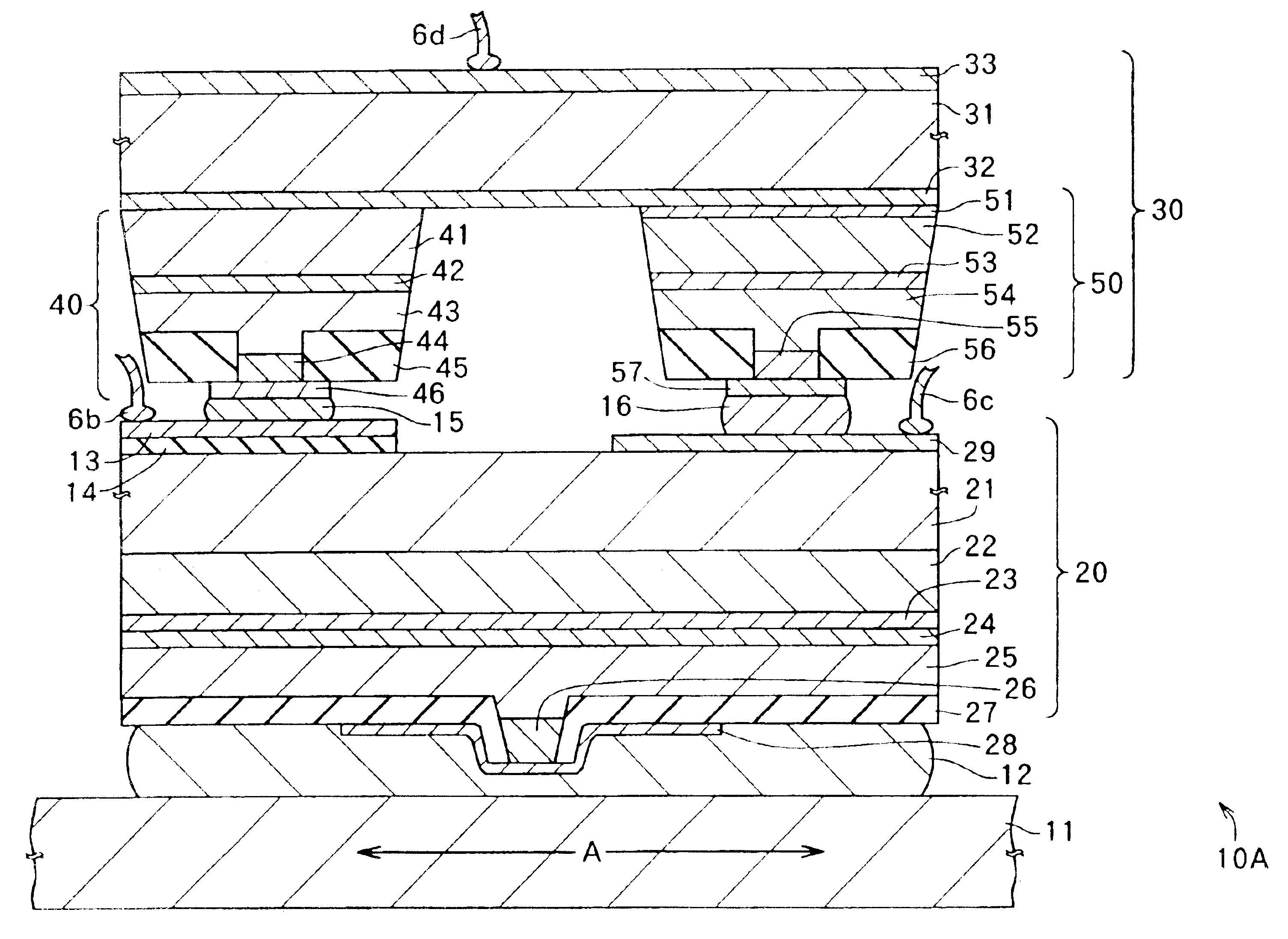
[0039]FIG. 4 shows the sectional structure of a light emitting device 10A according to a first embodiment of the invention. The light emitting device 10A has a supporting base 11, a first light emitting element 20 disposed on one face of the supporting; base 11, and a second light emitting element 30 disposed on the side of the first light emitting element 20 opposite to the supporting base 11.

[0040]The supporting base 11 is made of a metal such as copper (Cu) and serves as a heat sink for dissipating heat generated by the first and second light emitting elements 20 and 30. The supporting base 11 is electrically connected to an external power source (not shown) and also has the role of electrically connecting the first light emitting element 20 to the external power source.

[0041]The first light emitting element 20 is, for example, a semiconductor laser capable of emitting light having a wavelength of around 400 nm. The first light emitting element 20 has a configuration in which an ...

second embodiment

[0089]FIG. 11 shows a sectional structure of a light emitting device 10B according to a second embodiment of the invention. The light emitting device 10B has the same configuration, action, and effects as those of the light emitting device 10A except that a second light emitting element 60 is provided in place of the second light emitting element 30 in the light emitting device 10A in the first embodiment. The same reference numerals are given to the same components as those of the first embodiment and their detailed description will not be repeated.

[0090]The second light emitting element 60 in the second embodiment has the same configuration as that of the second light emitting element 30 except that a lasing portion 70 capable of emitting light having a wavelength in the band on the order of 500 nm (for example, 520 nm) is provided in place of the lasing portion 40 of the second light emitting element 30 in the first embodiment and the buffer layer 32 is not provided.

[0091]The las...

third embodiment

[0108]FIG. 17 shows a sectional structure of a light emitting device 10C according to a third embodiment of the invention. The light emitting device 10C has the same configuration, action, and effects as those of the light emitting device 10A of the first embodiment except that a first light emitting element 90 is provided in place of the first light emitting element 20 in the light emitting device 10A of the first embodiment, and a supporting base 17 is provided in place of the supporting base 11. The same reference numerals are given to the same components as those of the first embodiment and their detailed description will not be repeated here.

[0109]The first light emitting element 90 is largely different from the first light emitting element 20 with respect to the point that a different material is used for a first substrate 91. For example, the first substrate 91 is made of sapphire having a thickness of about 80 μm. Sapphire is an insulating material and is transparent in the ...


PUM


Abstract

A light emitting device which can be easily manufactured and can control the positions of light emission precisely, and an optical device. A first and second light emitting elements are formed on one face of a supporting base. The first light emitting element has an active layer made of GaInN mixed crystal on a GaN-made first substrate on the side thereof on which the supporting base is disposed. The second light emitting element has lasing portions on a GaAs-made second substrate on the side thereof on which the supporting base is disposed. Since the first and second light emitting elements are not grown on the same substrate, a multiple-wavelength laser having the output wavelength of around 400 nm can be easily obtained. Since the first substrate is transparent in the visible region, the positions of light emitting regions in the first and second light emitting elements can be precisely controlled by lithography.

Description

[0001]This application is a continuation of Ser. No. 09 / 783,914, filed Feb. 15, 2001.BACKGROUND OF THE INVENTION[0002]1. Field of the Invention[0003]The present invention relates to a light emitting device having a plurality of light emitting elements, and an optical device using the same.[0004]2. Description of the Related Art[0005]In recent years, in the field of light emitting devices, a semiconductor laser (LD; laser diode) in which a plurality of light emitting portions of different output wavelengths are formed on the same substrate (or board) (hereinafter referred to as a multiple-wavelength laser) is actively developed. An example of such a multiple-wavelength laser is, as shown in FIG. 1, obtained by forming a plurality of light emitting portions of different output wavelengths on a single chip (what is called a monolithic type multiple-wavelength laser). In the multiple-wavelength laser, for example, a lasing portion 201 formed by growing layers of semiconductor materials ...

Claims


Application Information

Patent Timeline
Patent Type & Authority Patents(United States)
IPC IPC(8): H01L25/075H01S5/40H01S5/00H01S5/323H01S5/02H01S5/022G02B6/42H01L33/06H01L33/08H01L33/28H01L33/32H01S5/02375H01S5/343
CPCB82Y20/00G11B7/1275H01L25/0753H01L25/0756H01S5/4043H04N9/315G11B2007/0006H01S5/02212H01S5/0224H01S5/02268H01S5/02272H01S5/02276H01S5/0425H01S5/2214H01S5/2231H01S5/32341H01S5/34326H01S5/34333H01S5/347H01S5/4087H01L2924/0002H01L2924/00H01S5/04256H01S5/02375H01S5/0237H01S5/02345H01S5/0234G02B6/42
Inventor IKEDA, MASAO
Owner SONY CORP
Why Eureka
Try Eureka