Method to monitor process charging effect

Inactive Publication Date: 2005-10-25
TAIWAN SEMICON MFG CO LTD
View PDF12 Cites 12 Cited by
  • Summary
  • Abstract
  • Description
  • Claims
  • Application Information

AI Technical Summary

Benefits of technology

[0011]A principle objective of the invention is to provide a simple and effective method for monitoring the effect of electron charging during the creation of a semiconductor device.
[0012]In accordance with the Objectives of the invention a new method is provided for monitoring the effect of electron charging during the creation of a semiconductor device.

Problems solved by technology

Continued accumulation of the electrical charges may result in creating an electromagnetic field in the region that is being charged of a magnitude large enough that molecular and structural damage may result in the accumulating layer.
The charge that accumulates on the ga

Method used


Image

  • Method to monitor process charging effect
  • Method to monitor process charging effect
  • Method to monitor process charging effect

Examples


Embodiment Construction

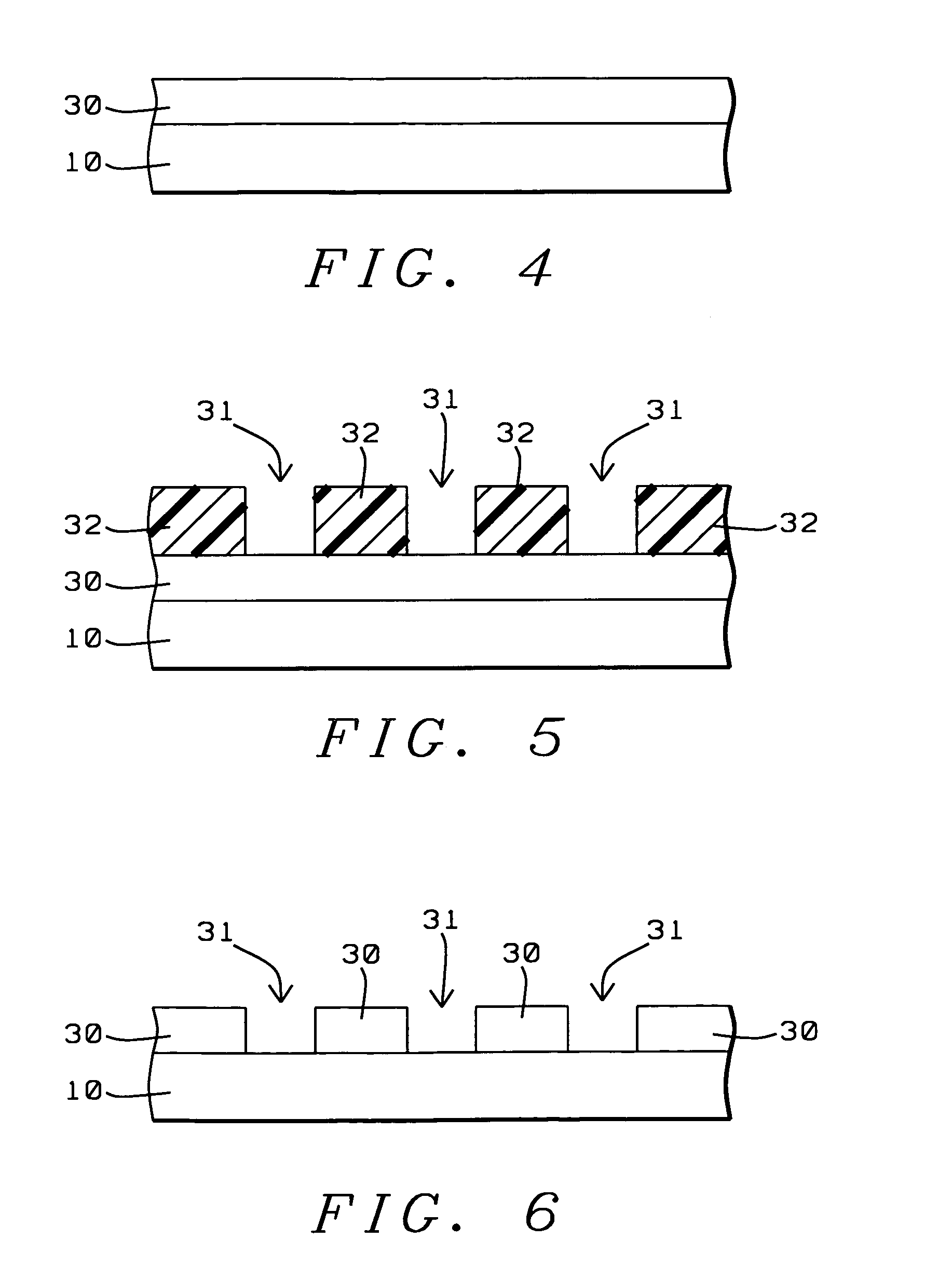
[0025]For a further understanding of the invention, basic concepts of EPROM device creation and the FN tunneling effect are first reviewed.

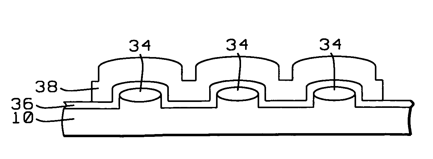
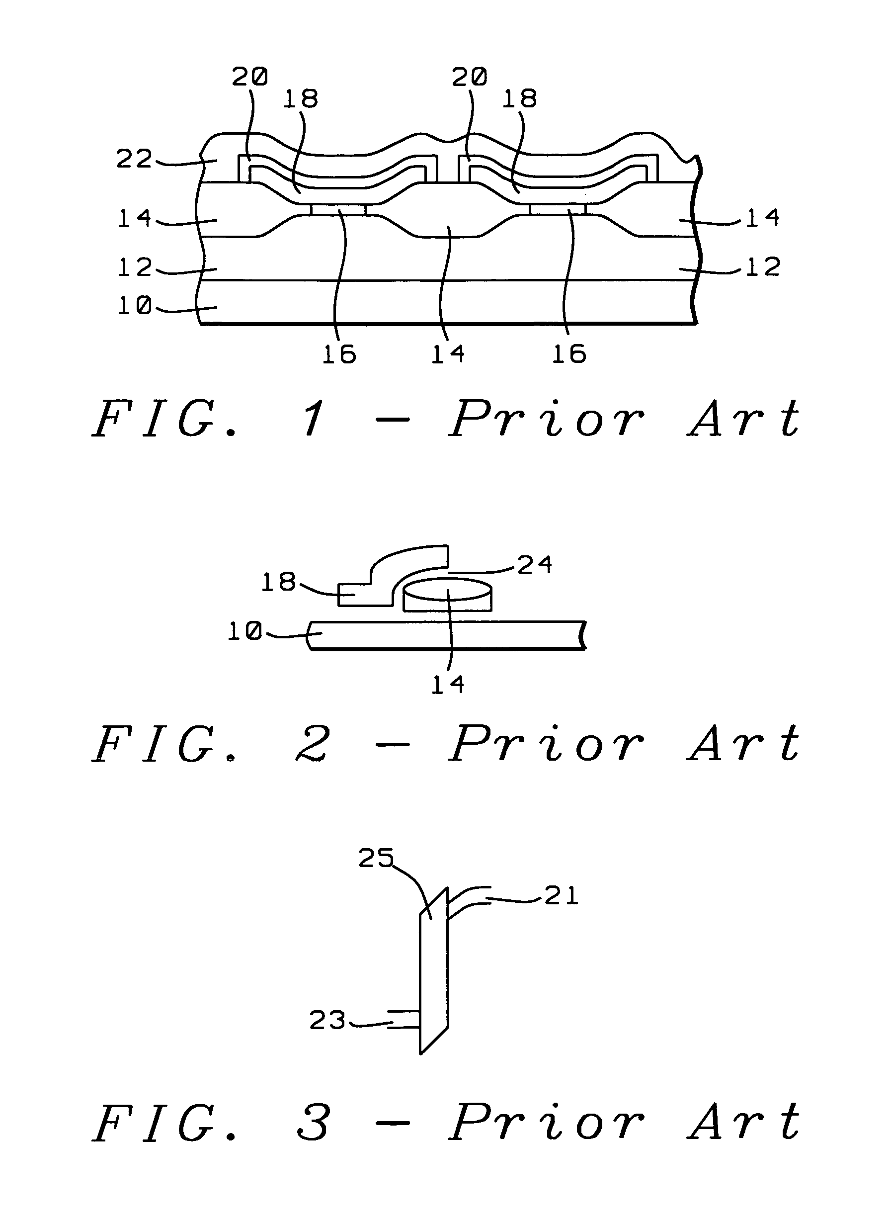
[0026]Referring for this purpose first to the cross section that is shown in FIG. 1, this cross section represents a conventional prior art NAND type EEPROM cell comprising the following elements:[0027]10, an n-type substrate over the surface of which the EPROM cell has been created[0028]12, a p-type impurity implant performed into the surface of substrate 10[0029]14, field isolation regions that electrically isolate adjacent gate structures and that typically are formed using LOCOS techniques[0030]16, layers of gate dielectric formed underneath the gate electrodes of the structure, tunneling current flows through these layers of gate dielectric during operation of the EERPROM cell[0031]18, the floating gates of the EEPROM cell[0032]20, a layer of insulating film that is created over the surface of the floating gates 18[0033]22, the control gate ...


PUM


Abstract

A new method is provided for monitoring the effect of electron charging during the creation of a semiconductor device. The method of the invention makes use of electron trapping that occurs as a result of FN tunneling in a layer of interlayer oxide of an EEPROM device. The electron trapping is monitored under conditions of processing. After the electron trapping has occurred, the rate of discharge of the trapped electron charge is measured during Wafer Acceptance Testing (WAT).

Description

BACKGROUND OF THE INVENTION[0001](1) Field of the Invention[0002]The invention relates to the fabrication of integrated circuit devices, and more particularly, to a method to monitor radiation induced charging effect during the creation of semiconductor devices.[0003](2) Description of the Prior Art[0004]During the creation of semiconductor devices, layers of semiconductor material are patterned and shaped to form separate elements of the devices. This patterning and shaping of the layers of semiconductor material typically requires the radiation of these layers by sources of high energy, whereby the energy that is imparted to the exposed layer determines the change that is affected in the exposed layer. Examples of such radiation are impurity implants that are performed in for instance the surface of a substrate in order to created regions of different conductivity in the exposed regions of the substrate. Well-known device features such as p-well and n-well impurities and the creat...

Claims


Application Information

Patent Timeline
IPC IPC(8): H01L21/66H01L21/8247H01L23/544H01L27/115
CPCH01L22/34H01L27/115H01L27/11521H01L22/10H01L2924/0002H01L2924/00H10B69/00H10B41/30
Inventor TZENG, JIANN-TYNGCHANG, YUH-HWACHEN, JIUN-NAN
Owner TAIWAN SEMICON MFG CO LTD
Why Eureka
Try Eureka