Shallow trench isolation process

a technology of isolation process and trench, applied in the direction of semiconductor devices, electrical equipment, transistors, etc., can solve the problems of affecting the inability to resist etchants used in subsequent processing, and the inability to detect the current of the transistor, etc., to achieve the effect of improving the performance of the transistor

Active Publication Date: 2005-11-01
TAIWAN SEMICON MFG CO LTD
View PDF63 Cites 229 Cited by
  • Summary
  • Abstract
  • Description
  • Claims
  • Application Information

AI Technical Summary

Benefits of technology

[0009]Trench structures, as well as other strain-inducing elements, are provided to induce strain in channel regions of trans

Problems solved by technology

Since the liner oxide contains Ge incorporated during the oxidation process, it may be more susceptible to attack by etchants used during subsequent processing, e.g., wet cleans such as h

Method used


Image

  • Shallow trench isolation process
  • Shallow trench isolation process
  • Shallow trench isolation process

Examples


Embodiment Construction

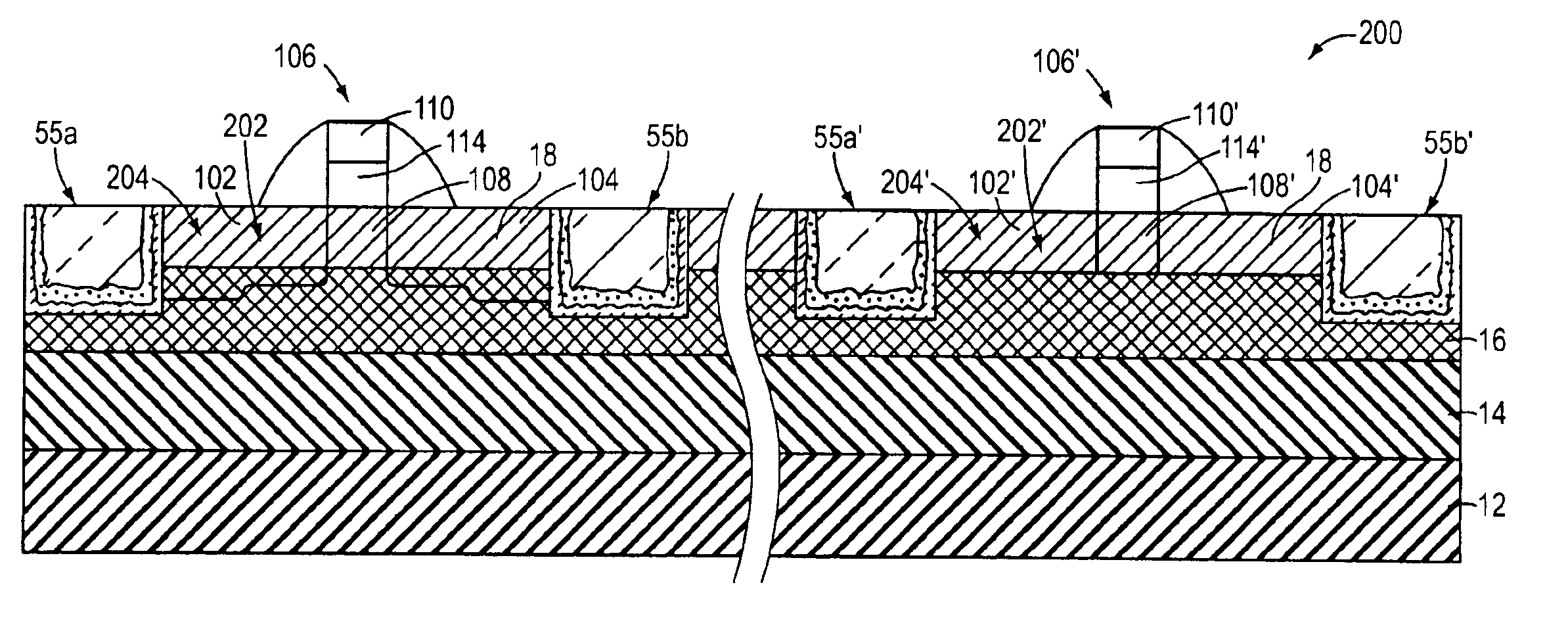
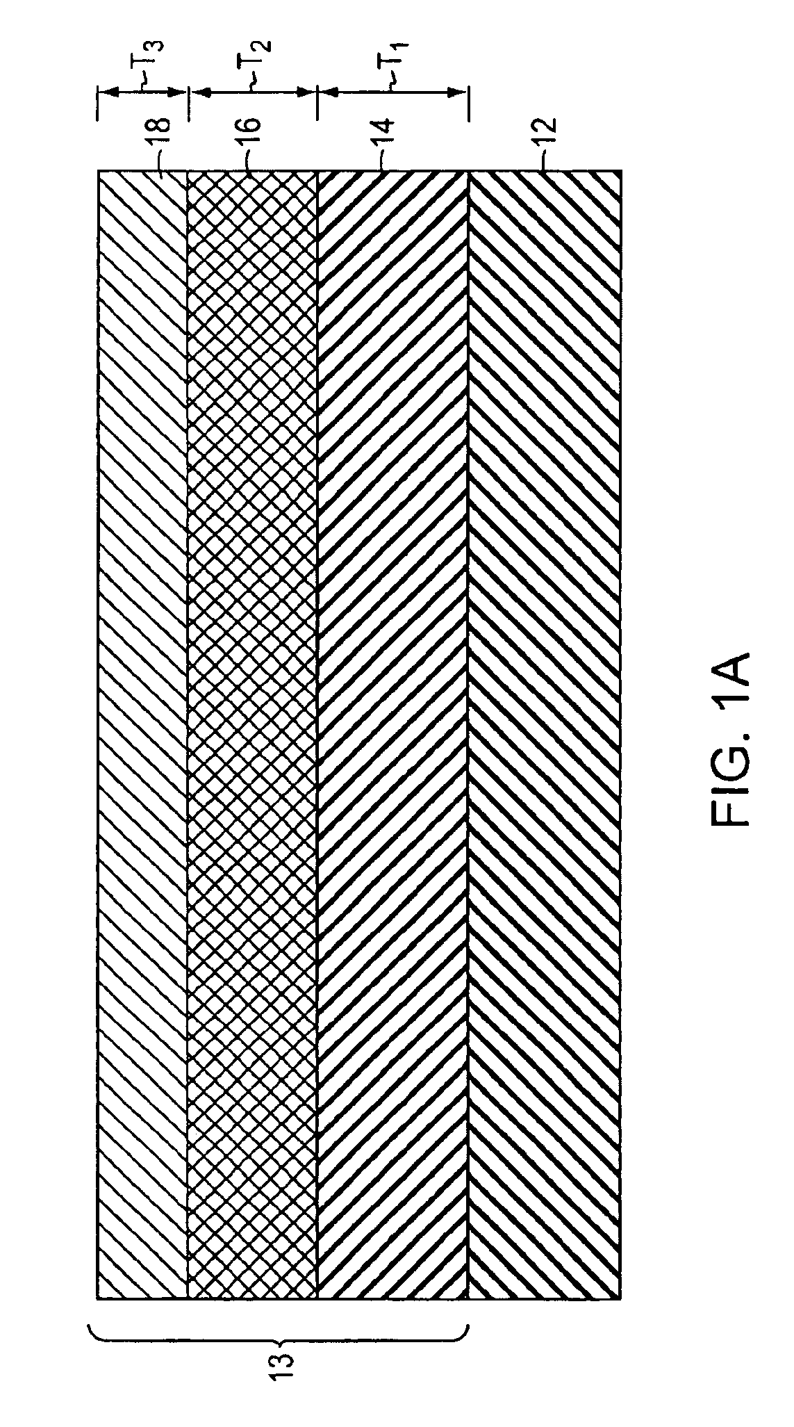
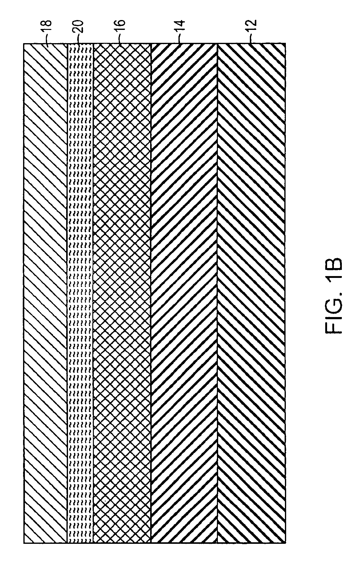
[0030]In FIG. 1a, which illustrates a structure amenable to use in connection with the present invention, a substrate 12 is made of a semiconductor, such as Si, Ge, or SiGe. A plurality of layers collectively indicated as 13 are formed on substrate 12. The plurality of layers 13 may include a relaxed graded buffer layer 14 disposed over substrate 12. Graded layer 14 includes, for example, SiGe having a grading rate of, for example, 10% Ge per μm of thickness, and a thickness T1 of, for example, 1-9 μm.

[0031]A relaxed layer 16 is disposed over graded SiGe layer 14. Relaxed layer 16 contains, for example, Si1-xGex wherein 0.1≦x≦0.9 and has a thickness T2 of, e.g., 0.2-2 μm. In some embodiments, Si1-xGex may include Si0.70Ge0.30 and T2 may be approximately 1.5 μm. Relaxed layer 16 may be substantially or fully relaxed, as determined by triple axis X-ray diffraction, and may have a threading dislocation density of 6 dislocations / cm2, as determined by etch pit density (EPD) analysis. Bec...


PUM


Abstract

A structure including a transistor and a trench structure, with the trench structure inducing only a portion of the strain in a channel region of the transistor.

Description

RELATED APPLICATION[0001]This application claims the benefit of U.S. Provisional Application 60 / 452,794 filed Mar. 7, 2003, the entire disclosure of which is hereby incorporated by reference.FIELD OF THE INVENTION[0002]This invention relates generally to semiconductor structures and particularly to shallow trench isolation.BACKGROUND[0003]The formation of integrated circuits includes the definition of isolation regions to prevent parasitic current leakage between devices. Isolation techniques include the shallow trench isolation (STI) scheme that has increased the planarity and packing density of silicon very large scale integration (Si VLSI) devices, and has thus been the isolation scheme of choice since approximately the 0.25 micrometer (μm) technology node.[0004]In a typical STI process, an active device area is protected by a pad oxide and a nitride overlayer, and isolation trenches are etched around the active device area. After the trench etch, a liner oxide is formed in each ...

Claims


Application Information

Patent Timeline
IPC IPC(8): H01L21/42H01L29/06H01L21/76H01L21/70H01L21/26H01L21/02H01L29/00H01L31/102H01L29/02H01L31/072H01L31/0328H01L31/0264H01L31/0336H01L31/06H01L31/109H01LH01L21/00H01L21/336H01L21/762H01L21/8234H01L21/8238H01L27/00H01L29/10H01L29/772
CPCH01L21/76224H01L21/823412H01L21/823807H01L21/823878H01L29/1054H01L29/6659H01L29/66628H01L29/66636H01L29/7842H01L29/785H01L21/76H01L21/762
Inventor CURRIE, MATTHEW T.LOCHTEFELD, ANTHONY J.
Owner TAIWAN SEMICON MFG CO LTD
Why Eureka
Try Eureka