Method and apparatus for continuous formation and lift-off of porous silicon layers

a technology of porous silicon and lift-off, applied in the field of microelectronics, can solve the problems of high cost of silicon wafer, loss of kerf, and high mechanical strength of separation layer, and achieve the effect of reducing the loss of kerf, and reducing the mechanical strength of separation layer

Inactive Publication Date: 2005-11-15
INTERUNIVERSITAIR MICRO ELECTRONICS CENT (IMEC VZW)
View PDF8 Cites 66 Cited by
  • Summary
  • Abstract
  • Description
  • Claims
  • Application Information

AI Technical Summary

Problems solved by technology

Most of the expensive silicon wafer provides mechanical strength to the cell.
This separation layer is a highly porous layer and is mechanically very weak.
These methods create kerf loss, need expensive equipment, are limited to removal of thick film layers, e.g., greater than 50 μm.

Method used


Image

  • Method and apparatus for continuous formation and lift-off of porous silicon layers
  • Method and apparatus for continuous formation and lift-off of porous silicon layers
  • Method and apparatus for continuous formation and lift-off of porous silicon layers

Examples


example 1

Experimental Setup

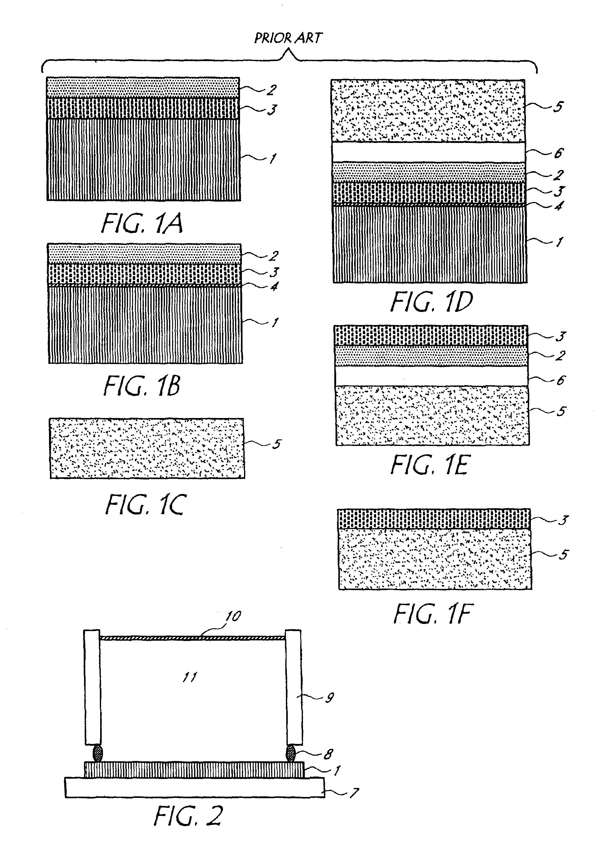
[0037]FIG. 2 illustrates the experimental set-up used for the porous silicon layer formation. Reference numeral 11 is the hydrofluoric acid solution. In the porous silicon formation the platinum electrode 10, which is resistant against hydrofluoric acid, acts as a negative electrode. The bottom plate 7 (e.g. stainless steel plate), which is in contact with the silicon wafer 1 (polished side up), acts as cathode. The rubber ring 8 prevents the outflow of the solution from the contact area of the Teflon® beaker 9 and wafer substrate 1. The rubber ring 8 is kept under pressure by the beaker 9, which in turn is pressurised by a stainless steel threaded ring (not shown).

example 2

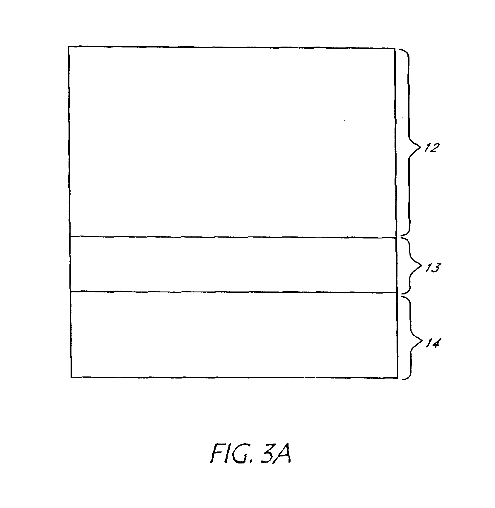
[0038]Experiments were carried out with a mixture of HF, acetic acid and deionised water in which the concentration of HF varies between the different experiments from 10% to 40% and current density varies from 25 mA / cm2 to 200 mA / cm2. The acetic acid is used as a wetting agent, and provides enough functionality to obtain a good pore distribution. Ethanol could also be used, but for environmental reasons acetic acid is preferred. For a given current density and for a given HF concentration, formation of the separation layer or a very high porosity layer or a detached layer as shown in FIG. 3A is obtained when the reaction is continued after a certain time. The low porosity layer 12, high porosity (separation) layer 13 just before lift-off and silicon wafer substrate 14 are visible on FIG. 3A. For a 25% HF solution and for 150 mA / cm2 current density this time is around 45-55 second and the thickness of the thin layer obtained is around 7 to 10 microns. Different layer thickness can b...

example 3

[0039]Electrochemical etching of silicon occurs at the HF solution / silicon interface when subjected to the flow of current. When a hole coming from the bulk silicon reaches to the interface, the Si—H bonds is replaced by Si—F bond due to an attack by a fluoride ion from the HF solution. The polarization induced by these Si—F bond lowers the electron density of the Si—Si bond and these are broken too. Silicon dissolves as tetravalent silicon fluoride (SiF4), which reacts with HF and produces fluorosilicic acid (H2SiF6). This electrochemical reaction is limited to the holes and results in pore formation. FIG. 4 illustrates the interface between bulk silicon and the HF solution where pore formation occurs. The numeral 15 indicates bulk silicon, 16 is the HF solution, 17 designates the holes, 18 are the fluoride ions and 19 is the interface.

[0040]Once the pore formation starts at a certain position, it goes straight down in silicon as shown in FIG. 5. The numeral 21 indicates bulk silic...


PUM

PropertyMeasurementUnit
current densityaaaaaaaaaa
thicknessaaaaaaaaaa
current densityaaaaaaaaaa

Abstract

A method and apparatus for slicing a semiconductor substrate. In one embodiment, the invention allows repetitive etching of a surface of the semiconductor substrate with a time dependent concentration of fluorine ions and a time dependent current I, such that multiple porous layers are obtained. The porous layer is released, and the released porous layer is removed from the surface of the substrate. The surface roughness of the porous layer is maintained within an acceptable or desired level of roughness value. The invention also provides an apparatus including a container having an etching solution. The semiconductor substrate may be protected by a tube covering at least a potion of said semiconductor substrate from said etching solution. The rate of insertion of said semiconductor substrate into the container is controlled to synchronize the lift-off with the insertion of the correct thickness of the semiconductor substrate. The anodising current is provided between two electrodes during operation.

Description

RELATED APPLICATIONS[0001]This application is a continuation-in-part, and hereby claims priority to and incorporates by reference the entire disclosure, of U.S. patent application Ser. No. 09 / 802,756, entitled “METHOD FOR THE FORMATION AND LIFT-OFF OF POROUS SILICON LAYERS”, filed on Mar. 9, 2001 now U.S. Pat. No. 6,649,485, which claims priority to U.S. Provisional Application No. 60 / 188,347, filed on Mar. 9, 2000 and to EP Application No. 00870040.3 filed Mar. 10, 2000.[0002]This application further claims priority to, and hereby incorporates by reference the entire disclosure of, U.S. Provisional Application No. 60 / 417,069, entitled “METHOD FOR THE CONTINUOUS FORMATION AND LIFT-OFF OF POROUS SILICON LAYERS”, filed on Oct. 8, 2002.BACKGROUND OF THE INVENTION[0003]1. Field of the Invention[0004]The present invention relates generally to the field of micro-electronics. More particularly, this invention relates to the formation of porous silicon layers (PSL) and their lift-off in the...

Claims


Application Information

Patent Timeline
Patent Type & Authority Patents(United States)
IPC IPC(8): H01L21/762H01L21/02H01L21/70H01L21/3063H01L21/306
CPCH01L21/3063H01L21/76259
Inventor SOLANKI, CHETAN SINGH
Owner INTERUNIVERSITAIR MICRO ELECTRONICS CENT (IMEC VZW)
Why Eureka
Try Eureka