Semiconductor device and method of fabricating the same

Inactive Publication Date: 2005-11-15
MICROSOFT TECH LICENSING LLC
View PDF14 Cites 21 Cited by
  • Summary
  • Abstract
  • Description
  • Claims
  • Application Information

AI Technical Summary

Benefits of technology

[0026](1) The present invention provides a semiconductor device comprising: a semiconductor substrate having a p-well and an n-well at a surface portion thereof; an insulation film formed on the semiconductor substrate and having an opening, at a bottom of which the p-well or n-well is exposed; a gate insulation film formed on the n-well or p-well exposed at the bottom of the opening; a first gate electrode including a first metal-containing film, which is formed in contact with the gate insulation film on the p-well and has a Fermi level on a conductive band side from a substantial center of a band gap of the semiconductor substrate, and a second metal-containing film formed on the first metal-containing film and having a lower resistance than

Problems solved by technology

However, a silicon oxide film, which is currently used as a gate insulation film, has a low dielectric constant, and thus the capacitance of the gate insulation film cannot be increased.
In addition, since a polysilicon used as a gate electrode has a high resistivity, it is difficult to decrease the resistance of the gate electrode.
However, these materials have drawbacks in that the heat resistance thereof is lower than that of currently used materials.
Thus, unlike the case of polysilicon gates, it is not po

Method used


Image

  • Semiconductor device and method of fabricating the same
  • Semiconductor device and method of fabricating the same
  • Semiconductor device and method of fabricating the same

Examples


Example

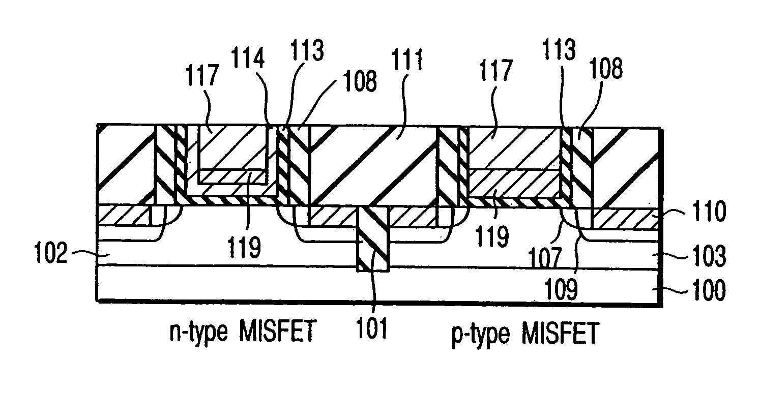
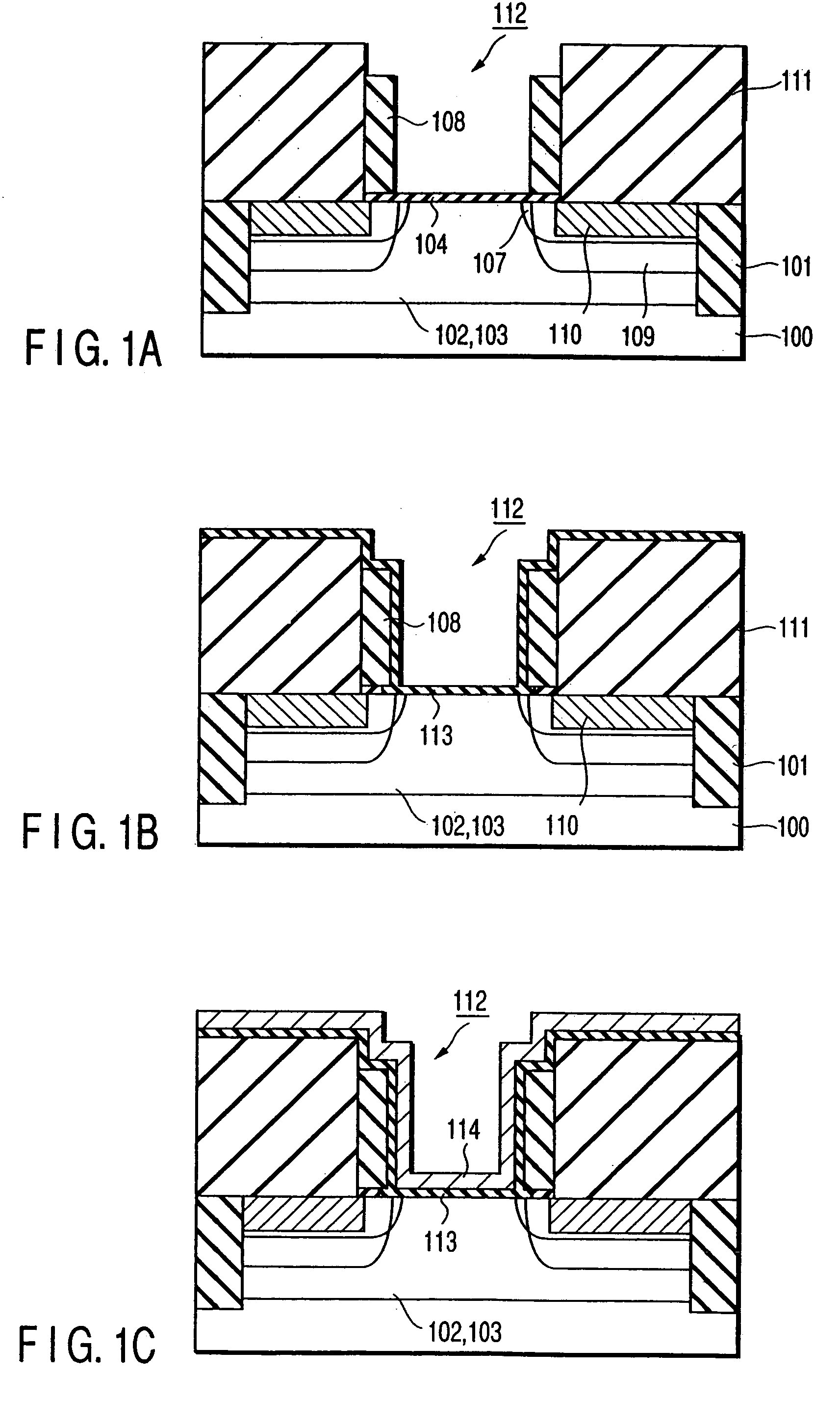
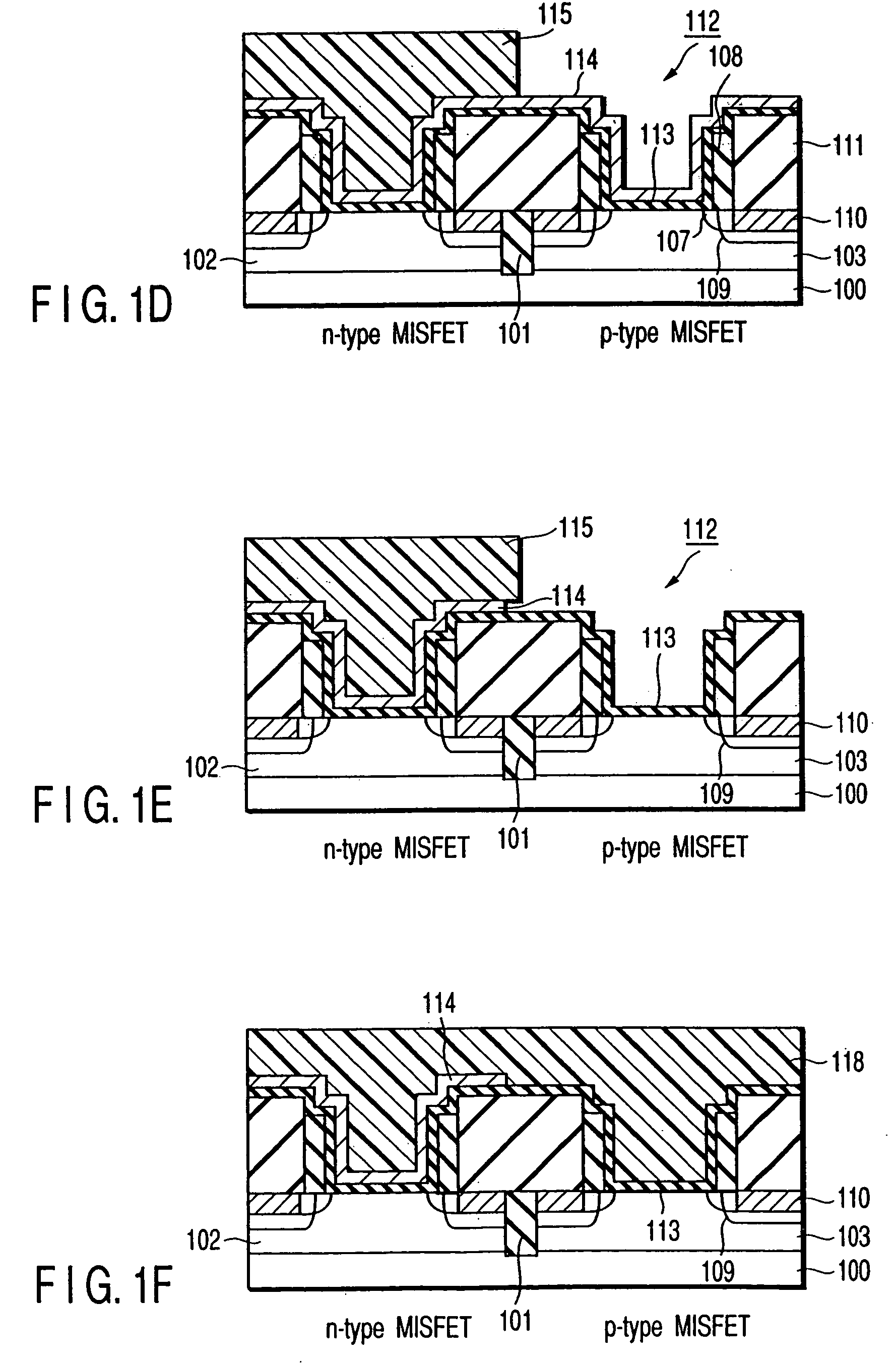
[0032]FIGS. 1A to 1I are cross-sectional views showing the steps of fabricating a semiconductor device according to an embodiment of the present invention.

[0033]A structure as shown in FIG. 1A is prepared through the prior-art fabrication steps shown in FIGS. 3A to 3D. A gate trench 112 is formed in a gate formation region by the interlayer film 111 and the gate side wall 18 formed of a second silicon nitride film with a width of about 40 nm on the silicon substrate 100, on which the silicide 110 of cobalt, titanium, etc. with a thickness of about 40 nm is formed on only the device isolation region 101, extension diffusion layer region 107, source / drain diffusion layer 109 and source / drain region. The dummy gate oxide film 104 is provided at the bottom of the gate trench 112.

[0034]In FIG. 1B, the dummy gate oxide film 104 at the bottom of the gate trench 112 is removed by a wet process using hydrofluoric acid, etc., thereby exposing the whole gate formation portion. A gate insulatio...


PUM


Abstract

A gate electrode of an n-type MIS transistor includes a first metal-containing film, which is formed in contact with a gate insulation film and has a Fermi level on a conductive band side from a substantial center of a band gap of a semiconductor substrate, and a second metal-containing film formed on the first metal-containing film and having a lower resistance than the first metal-containing film. A gate electrode of a p-type MIS transistor includes a conductive coating film, which is formed in contact with the gate insulation film and has a Fermi level on a valence band side from a substantial center of the band gap of the semiconductor substrate, and the second metal-containing film formed on the conductive coating film and having a lower resistance than the conductive coating film.

Description

CROSS-REFERECCE TO RELATED APPLICATIONS[0001]This application is a divisional of U.S. patent application Ser. No. 09 / 962,883, filed Sep. 25, 2001 now U.S. Pat. No. 6,737,309, the entire contents of which are incorporated herein by reference, and which is based upon and claims the benefit of priority from prior Japanese Patent Application No. 2000-293929, filed Sep. 27, 2000, the entire contents of which are incorporated herein by reference.BACKGROUND OF THE INVENTION[0002]1. Field of the Invention[0003]The present invention relates to a semiconductor device and a method of fabricating the same, and more particularly to an improvement of gate electrodes of an n-type MIS transistor and a p-type MIS transistor.[0004]2. Description of the Related Art[0005]Miniaturization of devices is indispensable in enhancing the performance of MIS transistors. However, a silicon oxide film, which is currently used as a gate insulation film, has a low dielectric constant, and thus the capacitance of t...

Claims


Application Information

Patent Timeline
IPC IPC(8): H01L21/336H01L21/70H01L21/02H01L21/8238H01L21/28H01L27/092H01L29/423H01L29/43H01L29/49H01L29/78
CPCH01L21/823842H01L29/66553H01L29/66583H01L2924/0002H01L2924/00H01L29/78
Inventor MATSUO, KOUJI
Owner MICROSOFT TECH LICENSING LLC
Why Eureka
Try Eureka