Cooling device, semiconductor laser light source device, semiconductor laser source unit, method of manufacturing semiconductor laser light source unit and solid state laser device

a cooling device and laser light source technology, applied in semiconductor laser arrangements, semiconductor lasers, lasers, etc., can solve the problems of reducing laser pumping efficiency, expensive manufacturing costs, and b>10/b> also having a problem in manufacturing yield, so as to reduce processing costs and achieve efficient cooling of semiconductor laser arrays.

Inactive Publication Date: 2005-11-29
MITSUBISHI ELECTRIC CORP
View PDF16 Cites 31 Cited by
  • Summary
  • Abstract
  • Description
  • Claims
  • Application Information

AI Technical Summary

Benefits of technology

[0035]A cooling device according to the present invention includes a first plate-like member made of metal, to which a cooled body is joined along the predetermined end portion, a second plate-like member made of metal, in which a cooling fluid introducing channel provided so as to reach an inlet opening portion, which introduces cooling fluid, and one end of an area connected to the inlet opening portion and corresponding to the end portion and a cooling fluid draining channel provided so as to reach an outlet opening portion, which drains cooling fluid, and the other end of the area connected to the outlet opening portion and corresponding to the end portion are formed, and a third plate-like member made of metal, which is formed along the area corresponding to the end portion and to which at least one cooling channel is provided through which cooling fluid flows in the longitudinal direction of the cooled body by communicating the cooling fluid introducing channel and the cooling fluid draining channel. Thus, the sectional area of the channel can be larger than that in the construction of the related art and the processing cost is reduced by comparison with the construction of the related art. The problems of blocking path with an extraneous matter and of high-pressure loss due to the path are overcome. Since the channel is provided along the longitudinal direction of the semiconductor laser array, the semiconductor laser array can be cooled efficiently.
[0036]Further, the plate-like member may be laminated alternately a plurality of times. The increase in the number of laminating layers allows more efficient cooling to be performed on the cooled body.
[0037]Furthermore, the second plate-like member may have a plurality of cooling channels provided in the vertical direction with respect to the longitudinal direction of the cooled body. As a result, the cooled body can be cooled efficiently by using the plurality channels each having larger sectional area than that in the construction of the related art.

Problems solved by technology

While a light source such as a xenon lamp is used for pumping the solid state laser in the related art, the output wavelength generally yields a broad spectrum, which reduces the laser pumping efficiency.
Since, in the cooling device 10 shown in FIG. 23, the micro-channel is formed on the silicon substrate by using the photo-lithography technology and the etching technology, expensive facilities such as an exposure device are needed, which causes a problem of expensive manufacturing costs.
Further, since the cooling device 10 has the silicon substrates, being used as the lamellas 1 and 3, or the insulator lamella 2, such as glass, which are mechanically weak, the cooling device 10 also has a problem in manufacturing yields.
Furthermore, since the lamellas 1 to 3 are mechanically weak, they cannot be fastened tightly when laminated.
Therefore, even when a gasket, such as silicon rubber, is used for sealing between the lamellas, water may leak in operations for a long period of time.
The cooling device 10 in FIG. 23 has a problem that laminating the lamellas 1 to 3 increases electric resistance.
However, the increase in serial electric resistance cannot be avoided, resulting in increase in Joule's heat generation.
Furthermore, the cooling device 10 in FIG. 23 does not use the other elements than the micro-channels efficiently.
Therefore, there is a problem that the cooling efficiency cannot be increased significantly.
However, the thermal conductivity of silicon is smaller than the thermal conductivity of metal.
Therefore, it is difficult to remove a heat amount generated by the heat conduction through the lamellas 1 and 3.
Additionally, since glass is used as the medium lamella 2, the heat conduction by the medium lamella 2 itself does not operate very well.
However, such a finer micro-channel is expensive in processing cost, and the path is easily blocked with dust.
As a result, the maintenance costs become higher, such as quality control over the cooling fluid.
Therefore, the problem of blocking the paths with dust in cooling fluid is not completely solved, and the precise water quality control is still required.
The effect of the temperature dependency of band gap energy results in a problem of uneven output wavelength among semiconductor lasers, which construct the semiconductor laser array.
Therefore, the capacity of a feeding unit for feeding a desired amount of flowing cooling fluid is increased, which also increases the device cost.

Method used


Image

  • Cooling device, semiconductor laser light source device, semiconductor laser source unit, method of manufacturing semiconductor laser light source unit and solid state laser device
  • Cooling device, semiconductor laser light source device, semiconductor laser source unit, method of manufacturing semiconductor laser light source unit and solid state laser device
  • Cooling device, semiconductor laser light source device, semiconductor laser source unit, method of manufacturing semiconductor laser light source unit and solid state laser device

Examples


embodiment 1

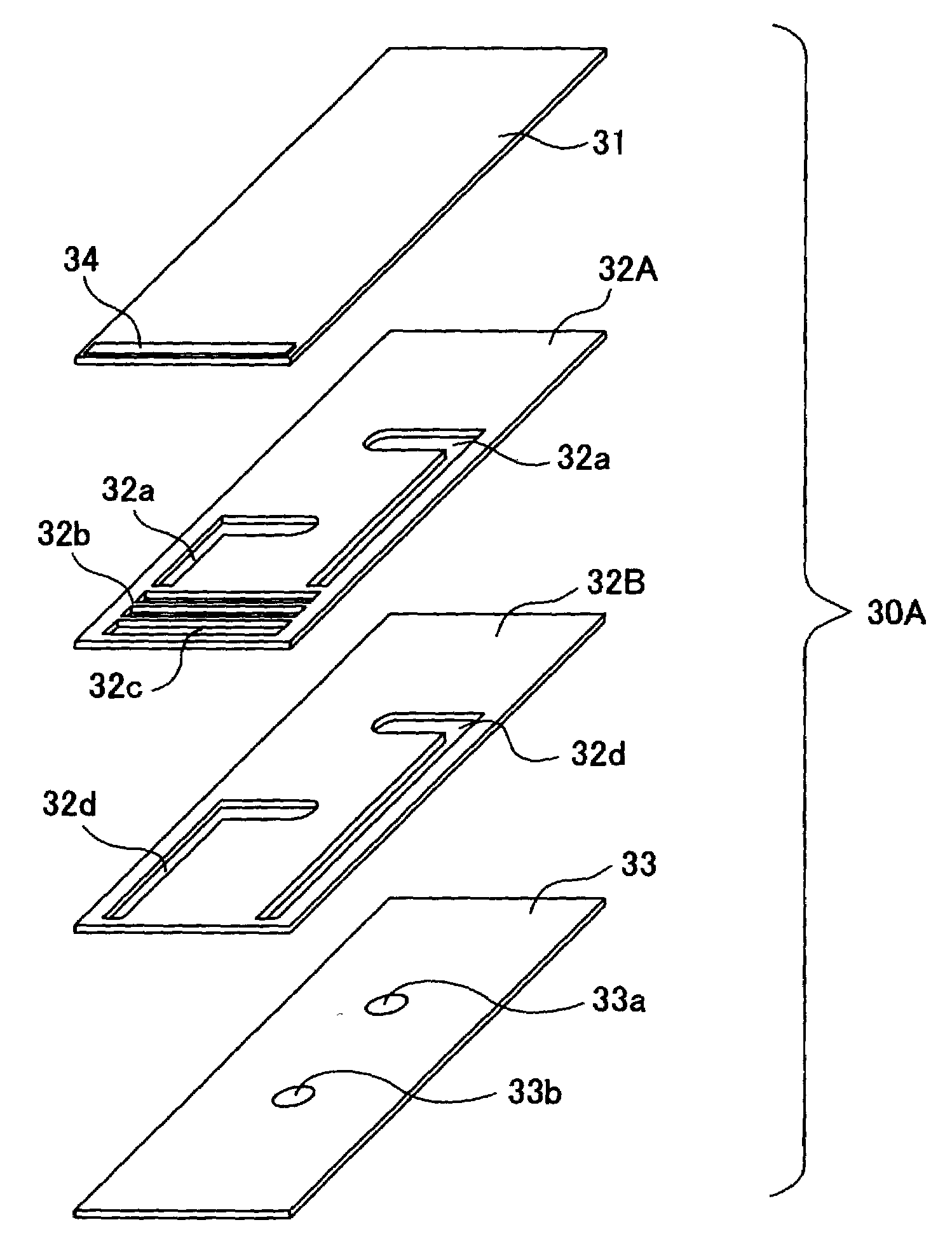
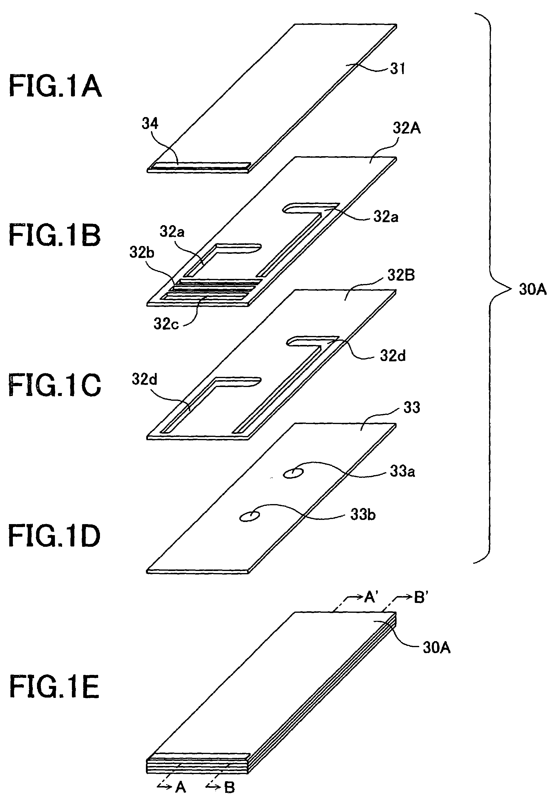
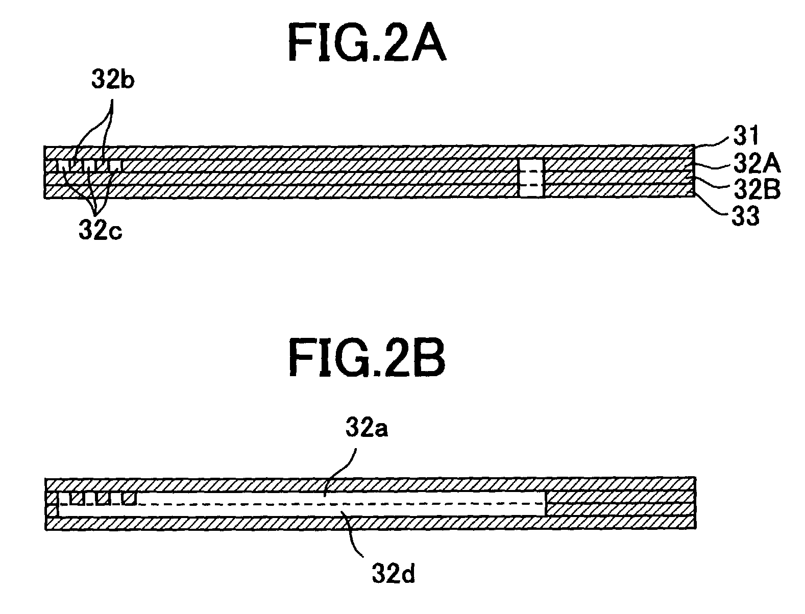
[0076]FIGS. 1A to 1D are exploded views each showing the construction of a cooling device 30A according to embodiment 1 of the present invention, and FIG. 1E is a perspective view showing a laminate constructed by members in FIGS. 1A to 1D. In FIGS. 1A to 1E, 31 refers to a plate-like member made of metal to which a semiconductor laser array 34, which is a cooled body, is connected. 32A and 32B refer to plate-like members in each of which a cooling channel functioning as a path for cooling fluid is formed. 33 refers to a plate-like member in which opening portions 33a and 33b are formed as a cooling fluid outlet and a cooling fluid inlet.

[0077]The thickness of the plate-like members 31 to 33 is determined based on the thickness of a laminate, the number of laminated layers, a pattern of a channel for constructing a cooling fluid flowing path, and so on. Typically, plate-like members in the order of 100 to 500 μm thick are selected, respectively.

[0078]Channels 32a and 32d, which func...

embodiment 2

[0095]In embodiment 1, a channel functioning as a cooling fluid flowing path is not formed in the plate-like member 32B at a position near a bottom surface of a position to which the semiconductor laser array 34 is connected. However, as shown in FIG. 5, a cooling channel 32e in slit shape, which is perpendicular to the flow of the cooling fluid in the cooling channel 32c of the plate-like member 32A may be formed in the plate-like member 32C at predetermined intervals.

[0096]FIG. 6A is a sectional view of a cooling fluid flowing path at a position where the cooling channel 32e in slit shape is formed in the cooling device 30C formed by using the plate-like member 32C, that is, a sectional view taken in the direction of the arrows substantially along the line E–E′ when plate-like members in FIG. 5 are laminated. FIG. 6B is a sectional view of a cooling fluid flowing path at a position where a divider 32f exists between adjacent, slit-shape cooling channels 32e, that is, a sectional v...

embodiment 3

[0101]FIGS. 9A to 9D is an exploded view showing the construction of a semiconductor laser light source device including a cooling device 30E according to embodiment 3 of the present invention. In FIG. 9, the same reference numerals as those in FIG. 1 are given to the same or like members as the cooling device according to embodiment 1, and the detail description will be omitted here.

[0102]In embodiment 3, the same members as those shown in embodiment 1 are used as the plate-like member 31, to which the semiconductor laser array 34 is connected, and the plate-like member 33, in which openings for the cooling fluid outlet and inlet are formed.

[0103]In FIG. 9B, a channel 32g, which functions as a path for introducing or draining cooling fluid, is formed near surfaces of both sides of the plate-like member 32D. The plate-like member 32D includes a cooling channel 32h, which is formed continuously with the channel 32g in the longitudinal direction of the semiconductor laser array 34 nea...


PUM


Abstract

A semiconductor laser light source device and light source unit according to the present invention include a first plate-like member made of metal, to which a semiconductor laser array is joined along the end portion, a second plate-like member made of metal, in which an inlet opening portion, which introduces cooling fluid, and a cooling fluid draining channel, and a third plate-like member made of metal, which is formed along the area corresponding to the end portion and to which at least one cooling channel is provided through which cooling fluid flows in the longitudinal direction of the semiconductor laser array by communicating the cooling fluid introducing channel and the cooling fluid draining channel. Thus, the sectional area of the channel can be larger than that in the construction of the related art and the processing cost is reduced by comparison with the construction of the related art. The problems of blocking path with an extraneous matter and of high-pressure loss due to the path are overcome. Since the channel is provided along the longitudinal direction of the semiconductor laser array, the semiconductor laser array can be cooled efficiently.

Description

TECHNICAL FIELD[0001]The present invention generally relates to a cooling device, and more particularly to a cooling device, which forcefully cools a semiconductor laser element with a higher density, a semiconductor laser light source device and semiconductor laser light source unit, both of which have the cooling device, a method of manufacturing the semiconductor laser light source unit, and a solid state laser device.BACKGROUND ART[0002]A semiconductor laser light source may be used mainly as a light source to be used for pumping a large output solid state laser. While a light source such as a xenon lamp is used for pumping the solid state laser in the related art, the output wavelength generally yields a broad spectrum, which reduces the laser pumping efficiency.[0003]When the pumping is performed by using a semiconductor laser having a sharp wavelength spectrum instead of the light source such as a xenon lamp, lasing can be occurred on the solid state laser with the higher eff...

Claims


Application Information

Patent Timeline
Patent Type & Authority Patents(United States)
IPC IPC(8): H01L23/473H01S3/0941H01S5/024H01S5/40
CPCH01L23/473H01S5/024H01S5/4025H01S3/0941H01S5/02423H01L2224/48091H01L2924/00014H01L21/4882
Inventor KITAYAMA, JIROFUKUMURA, KYOKOMATSUO, MITSUYASUSUGIYAMA, TORUHISAMORI, YOUICHI
Owner MITSUBISHI ELECTRIC CORP
Why Eureka
Try Eureka