High voltage MOS devices with high gated-diode breakdown voltage and punch-through voltage

a technology of diodes and high voltage, applied in the field of integrated circuits, can solve the problems of high voltage requirements of these technologies that cannot scale as easily, simultaneous requirements are often contradictory, and require the use of high voltages, so as to simplify the modeling of transistors, simplify design rules, and high punch-through characteristics.

Inactive Publication Date: 2005-12-06
ALTERA CORP
View PDF30 Cites 12 Cited by
  • Summary
  • Abstract
  • Description
  • Claims
  • Application Information

AI Technical Summary

Benefits of technology

[0008]It is desirable to provide a technique for obtaining a set of minimum channel length transistors in a CMOS technology for both high and low voltage use. The native high voltage transistors in the set should preferably maintain high punch-through characteristics. Preferably, the transistors in the set will have the same minimum channel length. Designing all the transistors in the set to the same minimum c

Problems solved by technology

However, some CMOS technologies, particularly those involving nonvolatile memory such as EEPROM, EPROM, Flash, antifuse technologies, and the like, require the use of high voltages internally.
The high voltage requirements of these technologies do not scale as easily as their

Method used


Image

  • High voltage MOS devices with high gated-diode breakdown voltage and punch-through voltage
  • High voltage MOS devices with high gated-diode breakdown voltage and punch-through voltage
  • High voltage MOS devices with high gated-diode breakdown voltage and punch-through voltage

Examples


Embodiment Construction

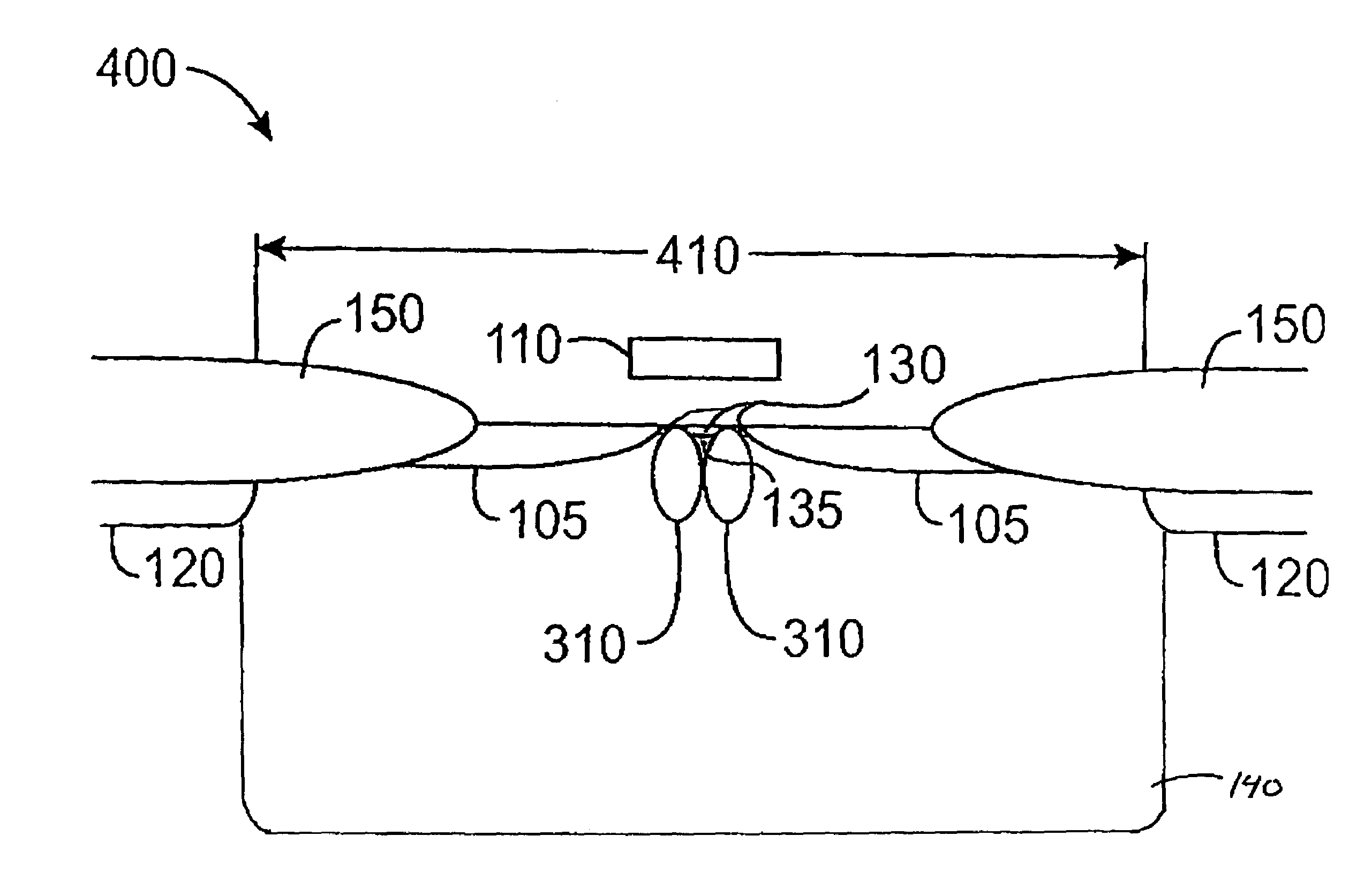
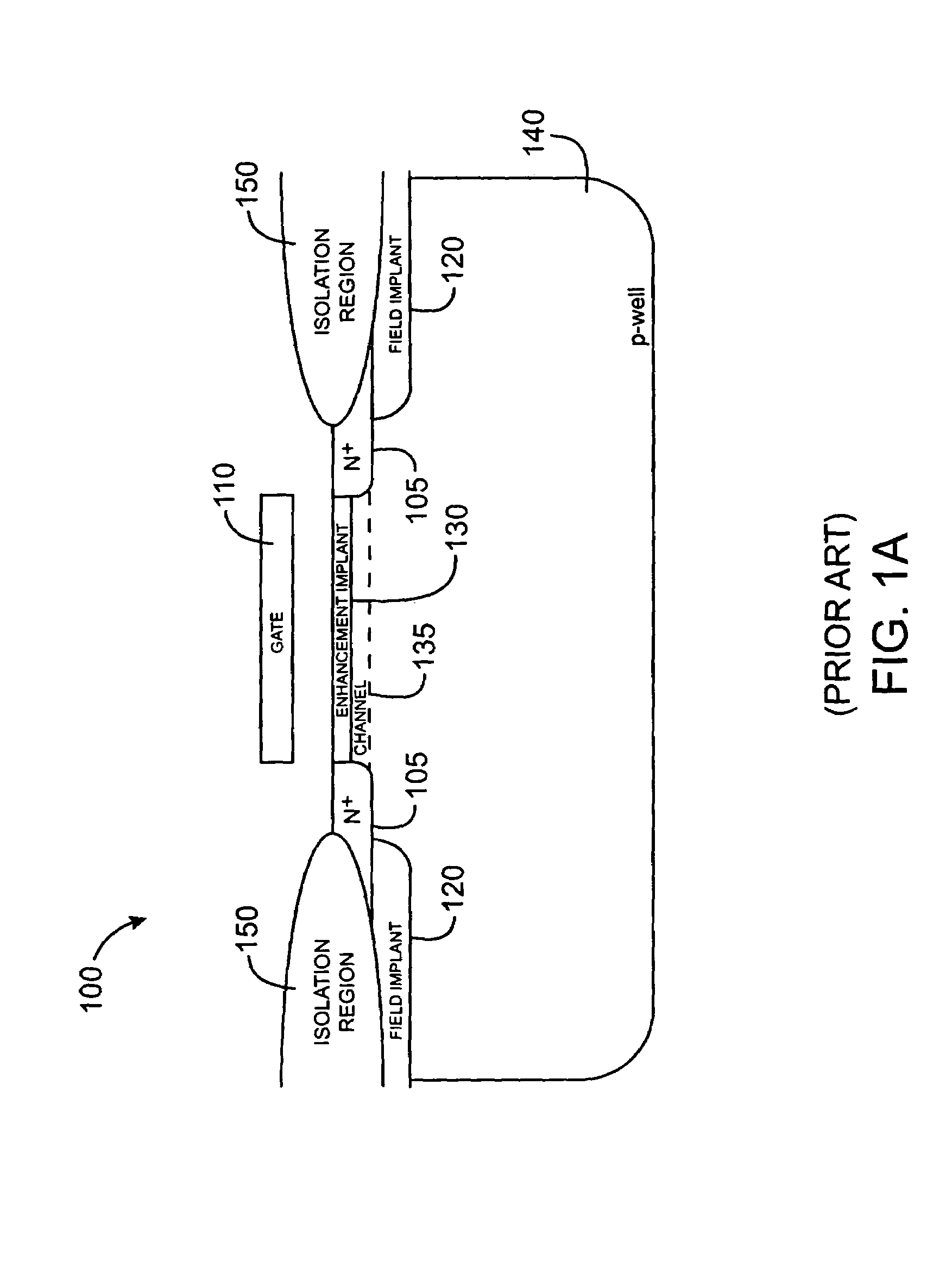
[0023]FIG. 1A shows a cross-section of a low voltage NMOS transistor 100. This transistor would be used in the implementation of typical logic gates on an integrated circuit. Transistor 100 has source / drain regions 105 made of n+ material and a polysilicon gate region 110. Operation of such a device is well known to those of skill in the art. Transistor 100 includes field implants 120 adjacent to the edge of each source-drain region 105. In addition, an enhancement implant 130 is formed in a channel region 135 of the transistor. Enhancement implant 130 is located close to the surface of the substrate and is used to adjust the magnitude of the threshold voltage Vt of the transistor to be about 0.50 volts to 0.70 volts. The transistor also has a well implant 140 of p-type material to control the body doping concentration of the device. An isolation region 150 electrically isolates individual devices from one another.

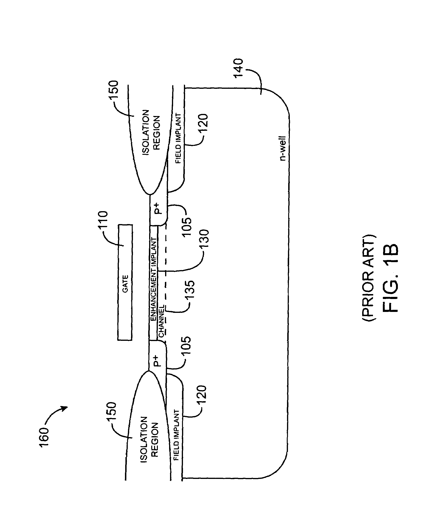
[0024]FIG. 1B shows a cross-section of a low voltage PMOS transistor ...


PUM


Abstract

A method of fabricating CMOS devices suitable for high voltage and low voltage applications, while maintaining minimum channel lengths for the devices. In one embodiment, pocket implants (310) are formed in a minimum channel device causing a reverse channel effect. The reverse channel effect is optimized for the minimum channel length of the device. Field implants (120), enhancement implants (130), and wells (140) are all formed using a single mask.

Description

CROSS-REFERENCE TO RELATED APPLICATIONS[0001]This application is a division of and claims the benefit of U.S. application Ser. No. 08 / 920,377, filed Aug. 29, 1997, now U.S. Pat. No. 6,417,550, which claims the benefit of Provisional Patent Application Ser. No. 60 / 024,927, filed Aug. 30, 1996, and Provisional Patent Application Ser. No. 60 / 025,843 filed Sep. 6, 1996, all of which are incorporated herein by reference for all purposes.BACKGROUND OF THE INVENTION[0002]The present invention relates to integrated circuits, and more particularly to high voltage CMOS transistors.[0003]A general trend in CMOS logic is to provide smaller transistors with minimum feature sizes and lower power supply voltages. This scaling of CMOS transistors allows for the incorporation of more devices onto the same area of silicon. It also allows for lower power operations and greater reliability because the electric field is reduced. As the power supply voltage is scaled down, peripheral requirements of the ...

Claims


Application Information

Patent Timeline
IPC IPC(8): H01L21/8238H01L27/105H01L29/10
CPCH01L21/823807H01L29/1083H01L27/105
Inventor MADURAWE, RAMINDA U.LIU, DAVID K. Y.
Owner ALTERA CORP
Why Eureka
Try Eureka