

Semiconductor device
a technology of semiconductor devices and semiconductors, applied in semiconductor devices, semiconductor/solid-state device details, electrical apparatus, etc., can solve the problems of large fluctuation of oxidation reaction rate, poor electric properties of silicon oxide films having a reduced film thickness, and difficult to realize a high-performance miniaturized transistor. , to achieve the effect of high reliability, superior characteristics and reliability
- Summary
- Abstract
- Description
- Claims
- Application Information
AI Technical Summary
Benefits of technology
Problems solved by technology
Method used
Image

Examples
first embodiment
(First Embodiment)
[0059]First, a description will be given of an oxide film formation at low temperatures by using plasma.
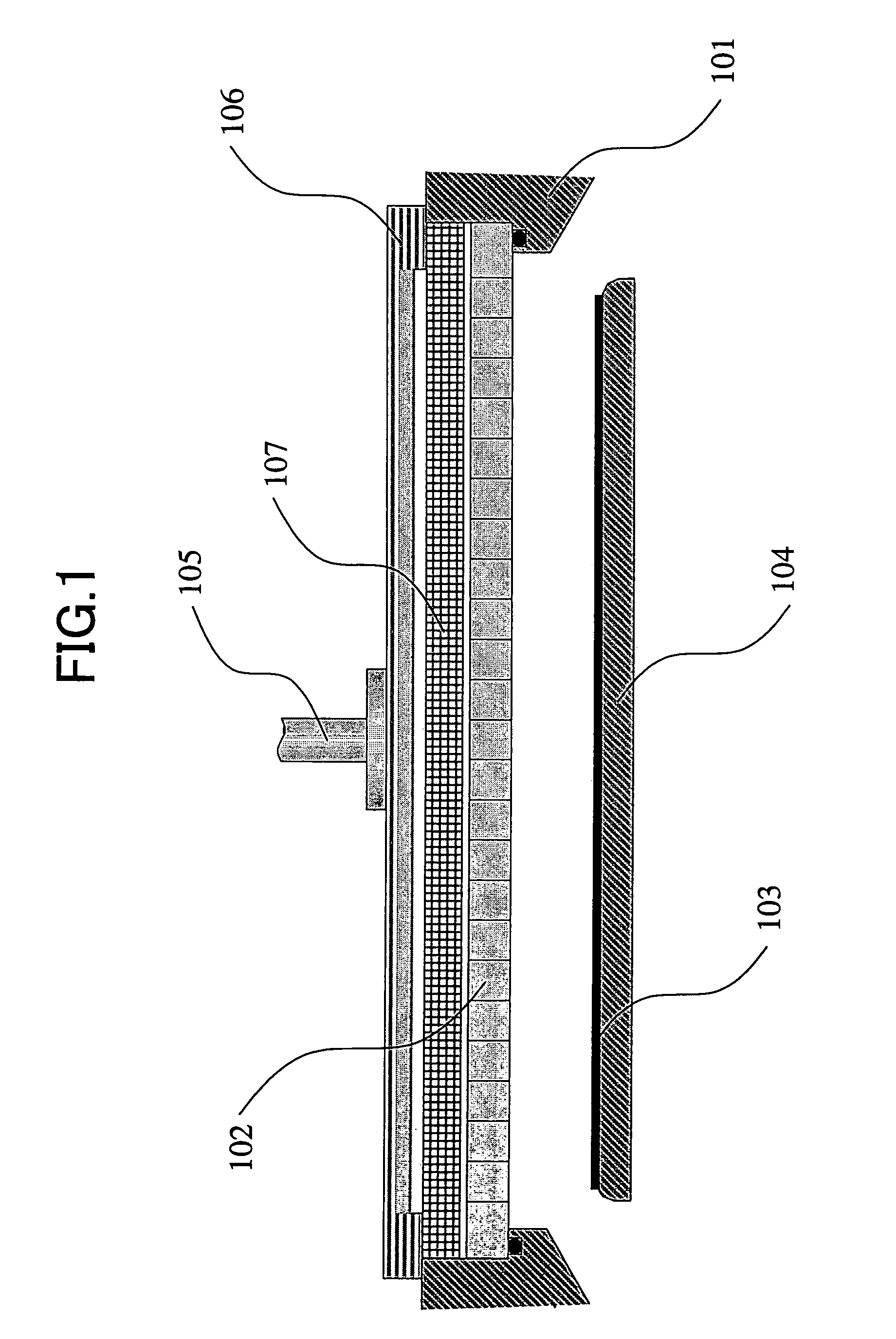
[0060]FIG. 1 is a cross-sectional view showing an example of a plasma processing apparatus used in the present invention and using a radial line slot antenna.
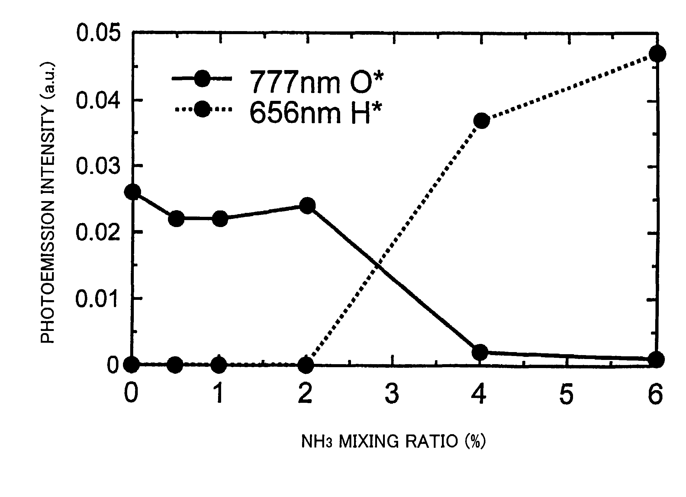
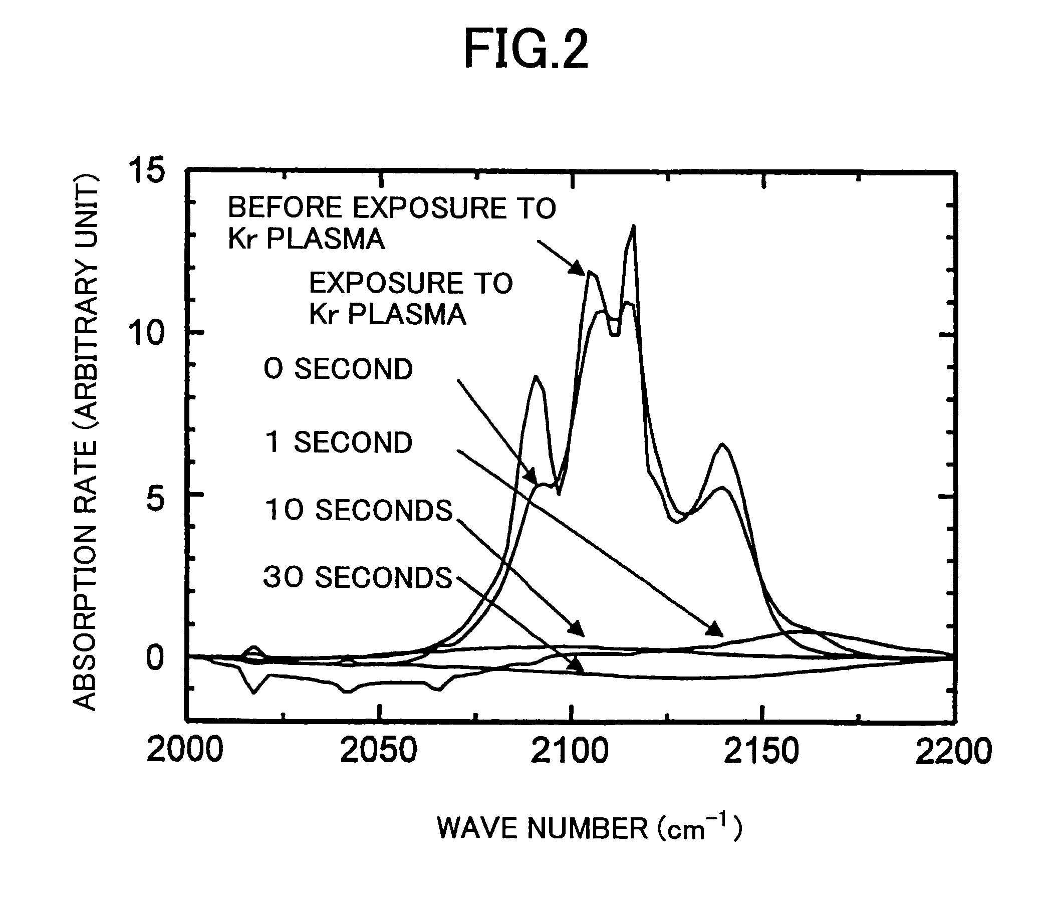
[0061]In this embodiment, in order to remove the hydrogen terminating the dangling bonds at a silicon surface, Kr, which is used as the plasma excitation gas in the subsequent oxide film formation process, is used, and the removal process of the surface-terminating hydrogen and the oxidation process are conducted in the same processing chamber continuously.
[0062]First, a vacuum vessel (processing chamber) 101 is evacuated and an Ar gas is introduced first from a shower plate 102. Then, the gas is changed to the Kr gas. Further, the pressure inside the processing chamber 101 is set to about 13.3 Pa (1 Torr).
[0063]Next, a silicon substrate 103 is placed on a stage 104 having a heating mechanism, and the temper...
second embodiment
(Second Embodiment)
[0090]Next, a description will be given of nitride film formation at low temperatures by using plasma. An apparatus similar to that shown in FIG. 1 is used for the nitride film formation.
[0091]In this embodiment, it is preferable to use Ar or Kr for the plasma excitation gas for removing the terminating hydrogen and for the nitride film formation, in order to form a high-quality nitride film.
[0092]Hereinafter, an example of using Ar will be represented.
[0093]First, the interior of the vacuum vessel (processing chamber) 101 is evacuated to vacuum and an Ar gas is introduced from the shower plate 102 such that the pressure inside the processing chamber is set to about 13.3 Pa (100 mTorr).
[0094]Next, the silicon substrate 103, subjected to hydrogenated water cleaning and the silicon dangling bonds at the surface are terminated by hydrogen in the preprocessing step immediately before, is introduced into the processing chamber 101 and is placed on the stage 104 having ...
third embodiment
(Third Embodiment)
[0111]Next, a description will be given of an embodiment that uses, for the gate insulation film, a two-layer structure of an oxide film and nitride film formed at a low-temperature by using plasma.
[0112]The formation apparatus of the oxide film and the nitride film used in this embodiment is identical with that of FIG. 1. In this embodiment, Kr is used for the plasma excitation gas for formation of the oxide film and the nitride film.
[0113]First, the vacuum vessel (processing chamber) 101 is evacuated to vacuum and an Ar gas is introduced into the processing chamber 101 from the shower plate 102. Then, the gas to be introduced the next is switched to the Kr gas from the initial Ar gas, and the pressure of the processing chamber 101 is set to about 133 Pa (1 Torr).
[0114]Next, the silicon substrate 103, subjected to diluted hydrofluoric acid treatment and the surface dangling bonds of silicon are terminated by hydrogen in the preprocessing step immediately before, i...
PUM
| Property | Measurement | Unit |
|---|---|---|
| temperature | aaaaa | aaaaa |
| thickness | aaaaa | aaaaa |
| temperature | aaaaa | aaaaa |
Abstract
Description
Claims
Application Information