

Capacitor, circuit board with built-in capacitor and method of manufacturing the same
a technology of built-in capacitors and capacitors, which is applied in the direction of printed capacitor incorporation, printed capacitor incorporation, printed electric component incorporation, etc., can solve the problems of uneven increase the number of steps, increase etc., and achieve high reliability, reduce the thickness of chemical polymerization film, and reduce the thickness of capacitors. the effect of the whole capacitor
- Summary
- Abstract
- Description
- Claims
- Application Information
AI Technical Summary
Benefits of technology
Problems solved by technology
Method used
Image

Examples
first embodiment
[0025]Referring to FIG. 1, the structure of a capacitor according to a first embodiment of the invention will be described in detail with an explanation of a method of manufacturing the same.
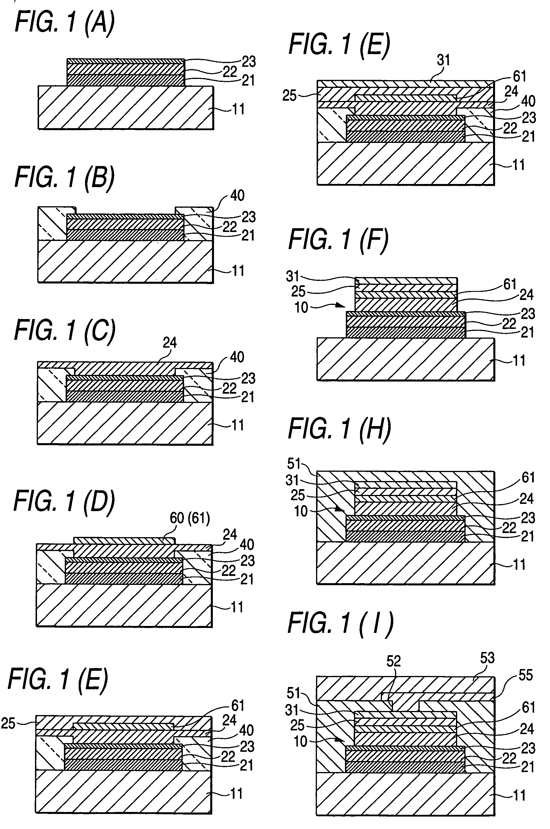
[0026]FIG. 1 is a sectional view showing steps in a method of manufacturing a polar capacitor and a circuit board with built-in capacitor according to the first embodiment of the invention. In the method of manufacturing a capacitor according to the embodiment, as shown in FIG. 1(A), a valve metal film 22 such as aluminum, tantalum, niobium, tungsten, vanadium, bismuth, titanium, zirconium, hafnium, their alloy or their compound (for example, niobium doped with oxygen) is formed on the surface of a first electrode 21 provided on a base material 11, and an anodic oxidation is then carried out to form a dielectric layer 23 constituted by an anodic oxide film (a dielectric layer forming step). In the embodiment, a tantalum film or a niobium film doped with oxygen is used as the valve metal film 22....
second embodiment
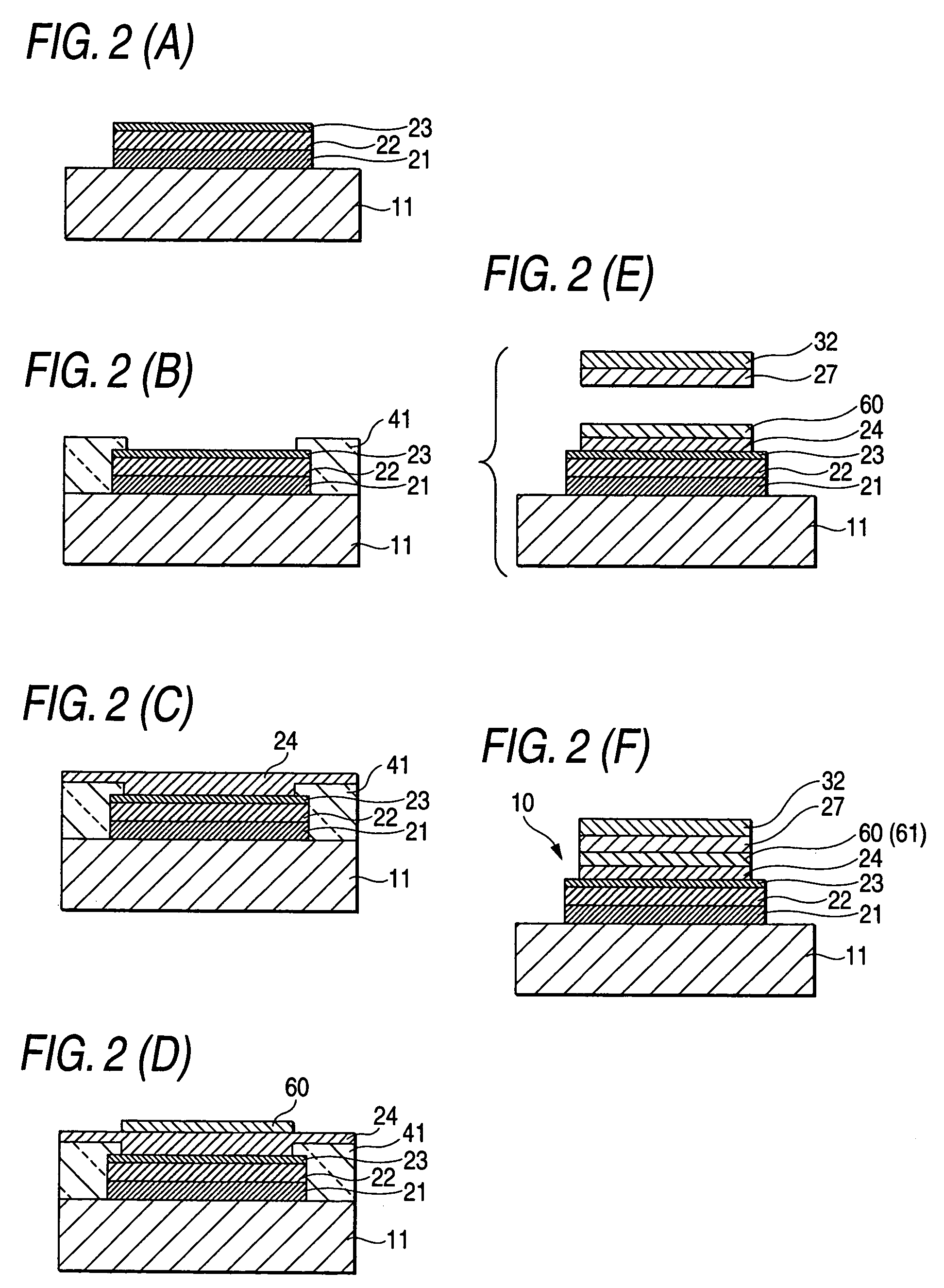
[0036]FIG. 2 is a sectional view showing steps in a method of manufacturing a polar capacitor according to a second embodiment of the invention. In the method of manufacturing a capacitor according to the embodiment, in the same manner as in the first embodiment, as shown in FIG. 2(A), a valve metal film 22 such as aluminum, tantalum, niobium, tungsten, vanadium, bismuth, titanium, zirconium, hafnium, their alloy or their compound (for example, niobium doped with oxygen) is formed on the surface of a first electrode 21 provided on a base material 11, and an anodic oxidation is then carried out to form a dielectric layer 23 constituted by an anodic oxide film (a dielectric layer forming step). In the embodiment, a tantalum film or a niobium film doped with oxygen is used as the valve metal film 22 in the same manner as in the first embodiment. The base material 11 is an insulating board for forming a circuit board with built-in capacitor which will be described below, and the first e...
third embodiment
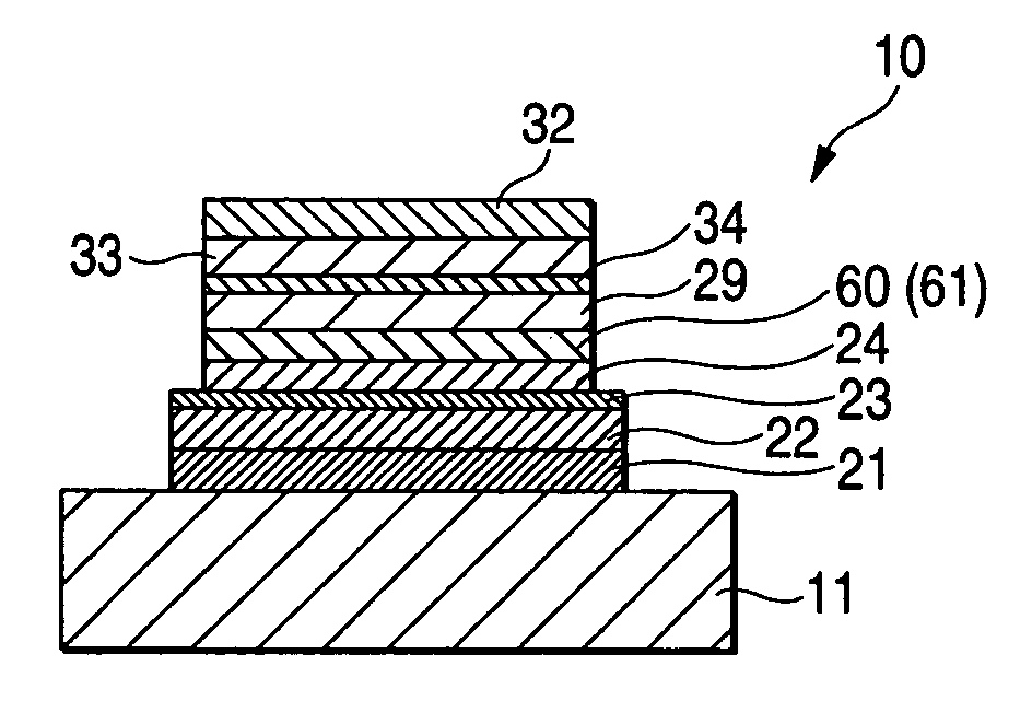
[0044]FIG. 3 is a sectional view showing steps in a method of manufacturing a polar capacitor according to a third embodiment of the invention. In the method of manufacturing a capacitor according to the embodiment, the steps shown in FIGS. 2(A) to 2(D) described in the second embodiment are carried out. Consequently, a valve metal layer 22, a dielectric layer 23, a chemical polymerization film 24 (a first solid electrolytic layer) and a paste-like conductive organic material 60 are provided on the surface of a first electrode 21 formed on a base material 11 as shown in FIG. 3(A).
[0045]Then, a second electrode 32 such as copper (Cu) and the surface of the first electrode 21 at a side on which the chemical polymerization film 24 and the paste-like conductive organic material 60 are formed are bonded to each other by a method such as hot press.
[0046]As shown in FIG. 3(B), thus, there is manufactured a capacitor 10 in which the first electrode 21, the valve metal layer 22, the dielectr...
PUM
| Property | Measurement | Unit |
|---|---|---|
| conductive | aaaaa | aaaaa |
| dielectric | aaaaa | aaaaa |
| conductivity | aaaaa | aaaaa |
Abstract
Description
Claims
Application Information