Group III nitride contact structures for light emitting devices

a technology of nitride and contact structure, which is applied in the direction of lasers, semiconductor lasers, semiconductor/solid-state device details, etc., can solve the problems of less likely transition, less functional constraints, and less likely leds

Inactive Publication Date: 2006-01-17
CREELED INC
View PDF27 Cites 21 Cited by
  • Summary
  • Abstract
  • Description
  • Claims
  • Application Information

AI Technical Summary

Problems solved by technology

Despite widespread use, LEDs are somewhat functionally constrained, because the color that a given LED can produce is limited by the nature of the semiconductor material used to fabricate the LED.
More common semiconductor materials such as silicon, gallium phosphide, or gallium arsenide are unsuitable for producing blue light because their bandgaps are approximately 2.26 eV or less, and in the case of silicon, are indirect semiconductors and inefficient light emitters.
When the conduction band minimum and valence band maximum do not have the same momentum state, a phonon (i.e., a quantum of vibrational energy) is required to conserve crystal momentum and the transition is called “indirect.” The necessity of a third particle, the phonon, makes indirect radiative transitions less likely, thereby reducing the light emitting efficiency of the device.
Although Group III nitrides offer a direct transition over a wide bandgap energy range, the material presents a particular set of technical manufacturing problems.
In particular, no commercially-viable technique has yet emerged for producing bulk single crystals of gallium nitride (GaN) that are capable of functioning as appropriate substrates for the gallium nitride epitaxial layers on which photonic devices would be formed.
Using different substrates, however, causes an additional set of problems, mostly in the area of crystal lattice matching.
As a result, when a gallium nitride epitaxial layer is grown on a different substrate, some crystal lattice mismatching and thermal expansion coefficient mismatching will occur.
Crystal lattice mismatches, and the strain they produce, introduce the potential for crystal defects.
This, in turn, affects the electronic characteristics of the crystals and the junctions, and thus tends to degrade the performance of the photonic device.
These kinds of defects are even more problematic in high power structures.
Furthermore, sapphire is insulating rather than conductive, and is unsuitable for conductivity doping.
In the absence of a conductive substrate, however, vertical devices cannot be formed.
This, however, tends to reduce the chemical and physical stability of the crystal.
In particular the generally wide bandgap of AlGaN tends to produce relatively poor ohmic contacts to p-type material.

Method used


Image

  • Group III nitride contact structures for light emitting devices
  • Group III nitride contact structures for light emitting devices
  • Group III nitride contact structures for light emitting devices

Examples


Embodiment Construction

[0035]The present invention is a p-type Group III nitride contact structure that is useful in light emitting devices capable of emitting in the red to ultraviolet portion of the electromagnetic spectrum.

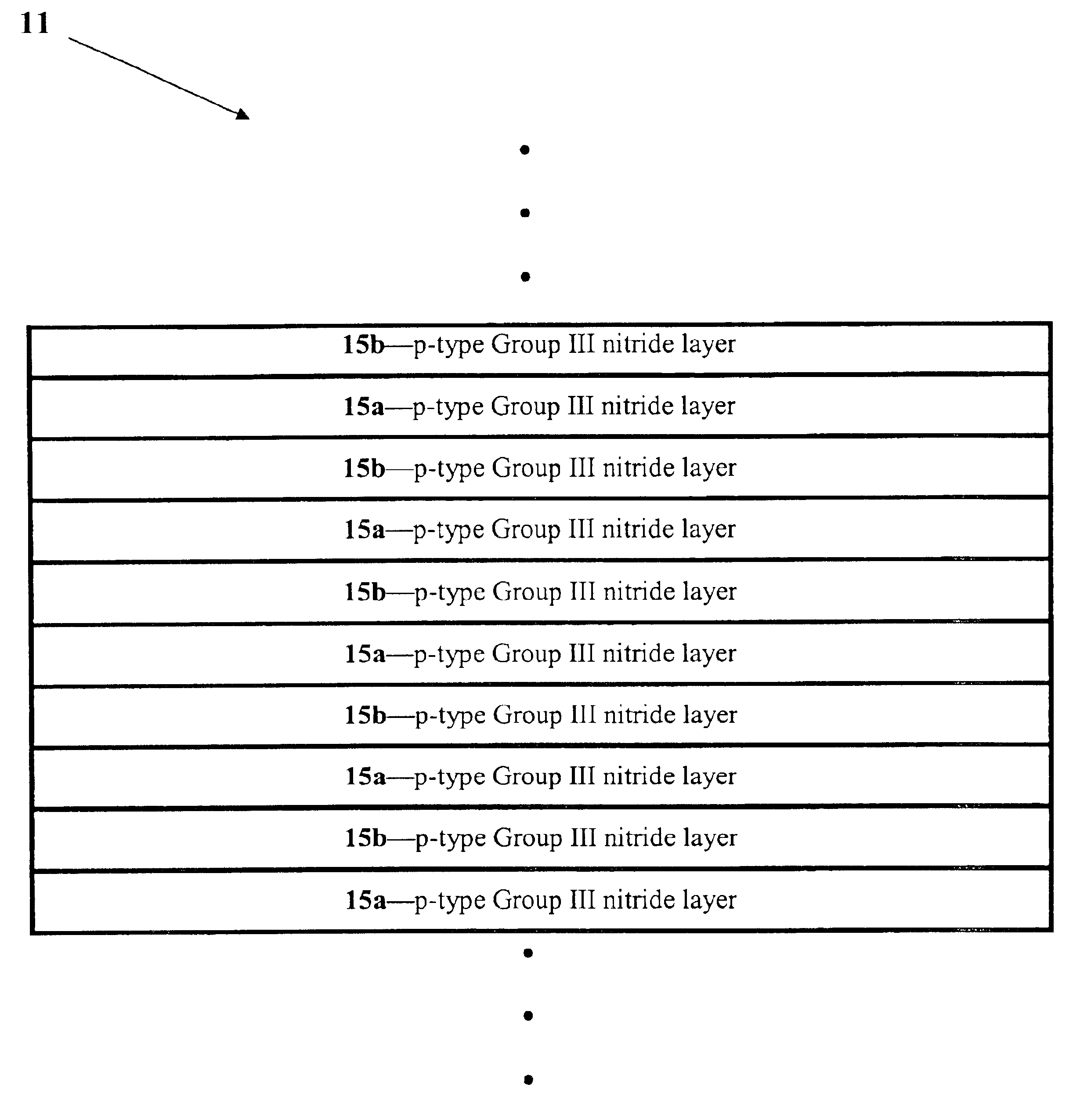
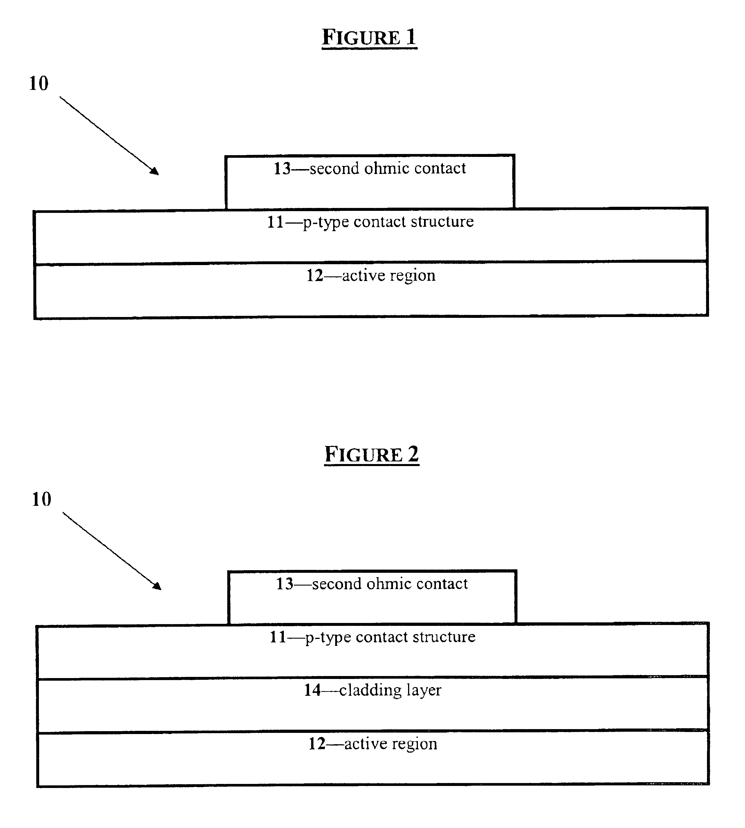
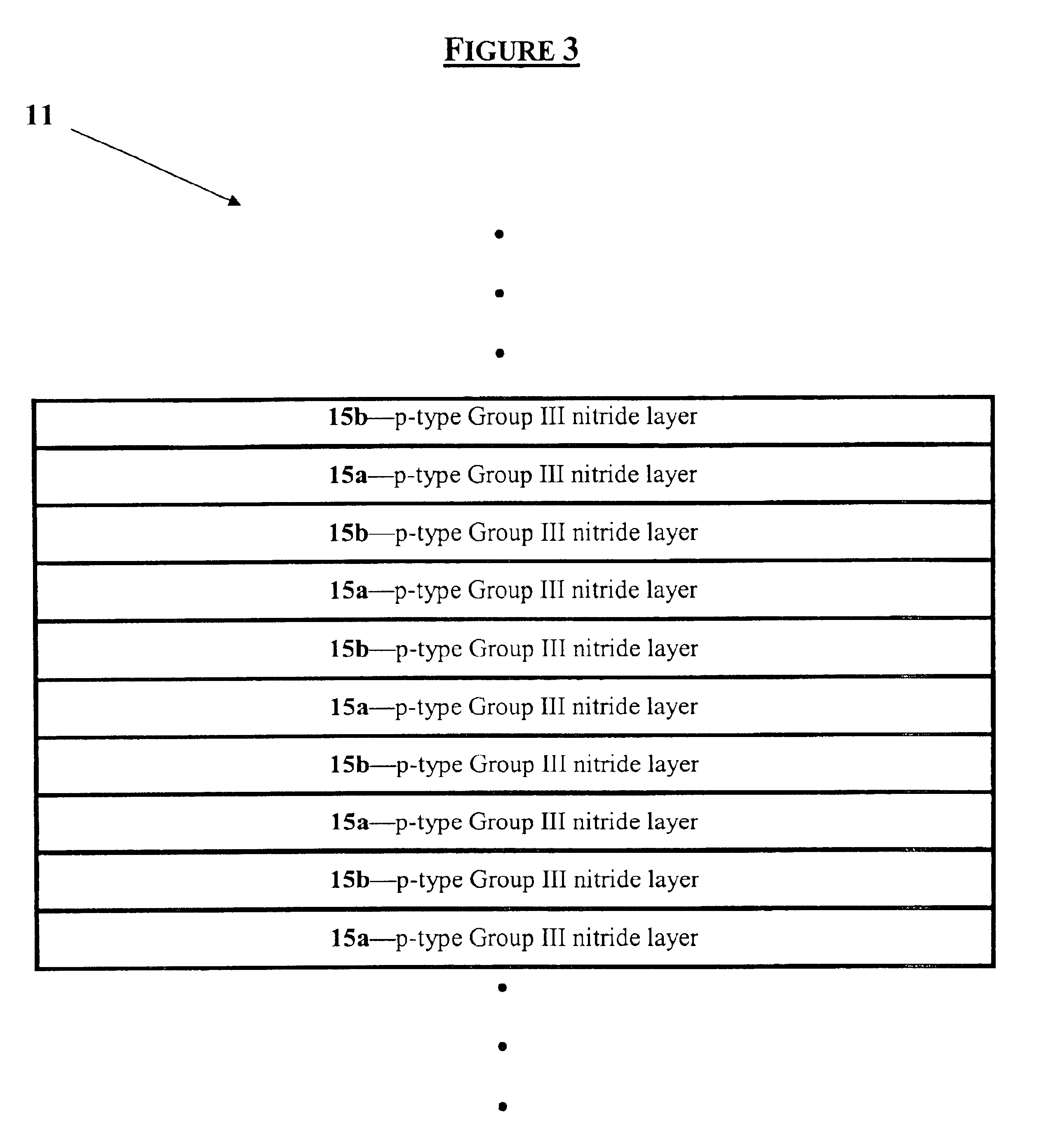
[0036]An understanding of the invention may be achieved with reference to FIGS. 1 and 2, each of which is a cross-sectional schematic view of an LED embodiment according to the present invention. The LED structure, which is generally designated at 10, includes a p-type contact structure 11 that is positioned between an active region 12 and an ohmic contact 13. See FIG. 1.

[0037]In another embodiment, the LED structure 10 further includes a cladding layer 14, which is positioned between the active region 12 and the p-type contact structure 11. See FIG. 2. Accordingly, in this embodiment, the p-type contact structure 11 is positioned between cladding layer 14 (as well as active region 12) and an ohmic contact 13.

[0038]It will be appreciated by those of ordinary skill in the art that, as...


PUM

PropertyMeasurementUnit
wavelengthsaaaaaaaaaa
optically transparentaaaaaaaaaa

Abstract

A superlattice contact structure for light emitting devices includes a plurality of contiguous p-type Group III nitride layers. The contact structure may be formed of p-type indium nitride, aluminum indium nitride, or indium gallium nitride. Also disclosed is a light emitting device that incorporates the disclosed contact structures.

Description

RELATED APPLICATIONS[0001]This application incorporates entirely by reference the following co-pending and commonly-assigned applications: Ser. No. 09 / 706,057 (Group III Nitride Light Emitting Devices with Gallium-Free Layers), filed on Nov. 3, 2000 and issued as U.S. Pat. No. 6,534,797; Ser. No. 09 / 760,635 (Group III Nitride LED with Undoped Active Layer and Undoped Cladding Layer), filed on Jan. 16, 2001); and Ser. No. 10 / 365,901 (Group III Nitride LED with Silicon Carbide Cladding Layer, filed on Feb. 13, 2003). This application claims priority, pursuant to 37 C.F.R. 1.78, to Ser. No. 10 / 376,494 (Light Emitting Devices with Group III Nitride Contact Layer and Superlattice), filed on Mar. 1, 2003 with a priority date of Nov. 3, 2000. This application also claims priority to Ser. No. 09 / 760,635, filed on Jan. 16, 2001.FIELD OF THE INVENTION[0002]The present invention relates to Group III nitride contact structures that can be included in light emitting devices, particularly light e...

Claims


Application Information

Patent Timeline
Patent Type & Authority Patents(United States)
IPC IPC(8): H01L33/00H01L33/04H01L33/14H01S5/042H01S5/323H01S5/34
CPCB82Y20/00H01L33/04H01S5/0425H01S5/32341H01L33/14H01S5/3425
Inventor EDMOND, JOHN ADAMDOVERSPIKE, KATHLEEN MARIEBERGMANN, MICHAEL JOHNKONG, HUA-SHUANG
Owner CREELED INC
Why Eureka
Try Eureka