Circuit design for a circuit for switching currents

a circuit design and switching current technology, applied in the direction of electric variable regulation, process and machine control, instruments, etc., can solve the problems of increasing overvoltage occurring at unable to guarantee the low-inductance linkage of the power semiconductor device to the dc link capacitor in all cases, etc., to shorten the transient switch-off operation of the power semiconductor device, shorten the current conductor arrangement, and reduce the inductance and ohmic resistance of the current conductor

Inactive Publication Date: 2006-01-24
VITESCO TECH GERMANY GMBH
View PDF11 Cites 11 Cited by
  • Summary
  • Abstract
  • Description
  • Claims
  • Application Information

AI Technical Summary

Benefits of technology

[0006]The object of the invention is to create a circuit design for switching currents which can be used where space is at a premium and can be mass-produced at low cost levels, and permit both a low-inductance and also a low-resistance connection of the power semiconductor devices to a DC link, and a low-resistance connection to one or more DC link capacitors.
[0011]This measure serves to reduce the inductance and ohmic resistance of the current conductor arrangement (main and ancillary current conductors connected in parallel), a shortening of the transient switch-off operation of the power semiconductor devices is achieved, and the energy converted in the power semiconductor devices during the switch-off operation is also less—the power loss is reduced—and the heat is better distributed throughout the entire switching cycle.

Problems solved by technology

However, this is only possible in the case of simple arrangements of DC link capacitors and power semiconductor devices.
If additional components such as gate resistors are required, a low-inductance linkage of the power semiconductor devices to the DC link capacitors can no longer be guaranteed in all cases because the current-carrying copper surfaces are “cut” by the resistors and thus their resistance and inductance are increased.
As leakage inductances become greater, the overvoltage occurring at the power semiconductor devices increases.

Method used


Image

  • Circuit design for a circuit for switching currents
  • Circuit design for a circuit for switching currents
  • Circuit design for a circuit for switching currents

Examples


Embodiment Construction

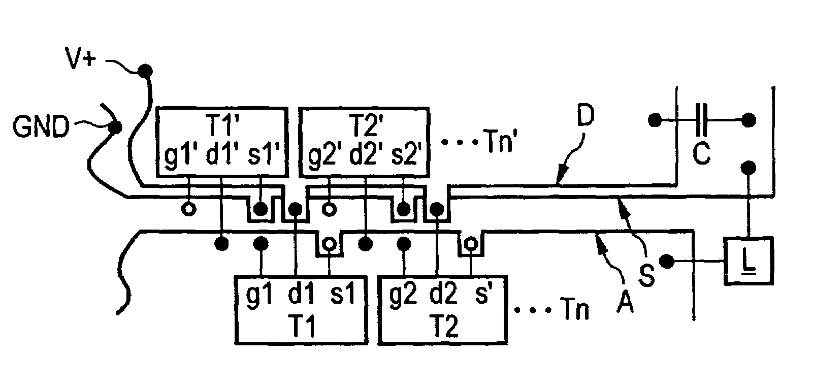
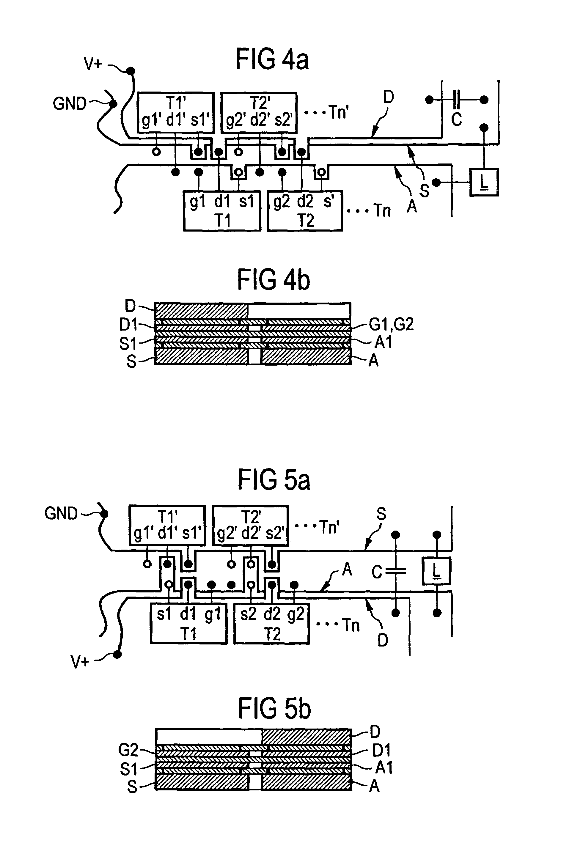
[0020]Where the following refers to a current conductor, this can be a conducting wire, a printed circuit board, a leadframe, a bus bar or similar. With regard to the following exemplary embodiments, for the sake of simplicity the current conductors should take the form of already known printed circuit boards (current-conducting layers applied to an electrically insulating substrate material) for example.

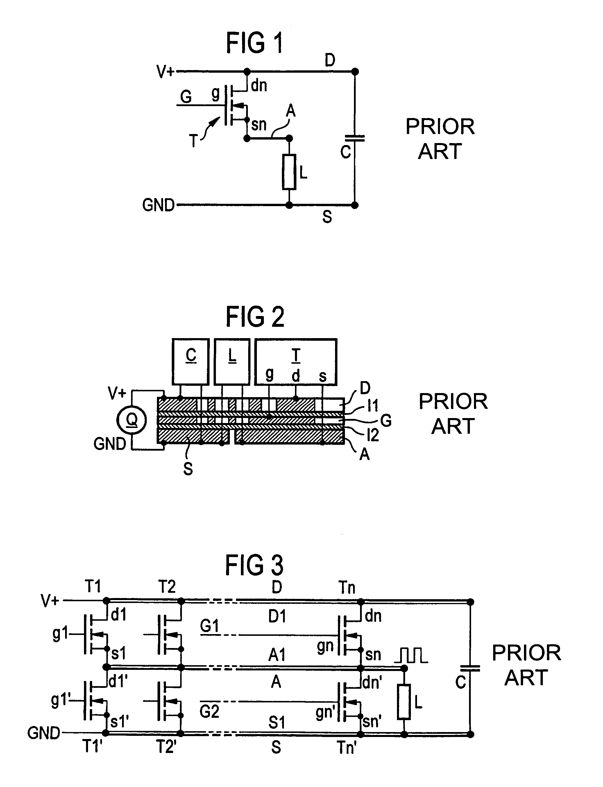
[0021]FIG. 1 shows a known circuit for controlling a load L which is applied in series with a switch element T, normally a power semiconductor device taking the form of a bipolar transistor or MOSFET, to the poles V+ and GND of an energy source. If the switch element is switched in quick succession, a DC link capacitor C connected in parallel with the series circuit comprising switch element T and load L is required.

[0022]The current conductors by means of which the elements T, L and C are interconnected and connected to the energy source are denoted by D, A, S and G. The gate termi...


PUM


Abstract

A circuit design for a circuit for switching currents is disclosed, comprising at least one switch element (T1 . . . Tn, T1′ . . . Tn′), and at least one respective main current conductor (D, S, A) for interlinking the switch element, the poles (V+, GND) of a current source and an energy accumulator (C). The aim of the invention is to reduce ohmic resistance and inductive resistance of such a circuit. To this end, an ancillary current conductor (D1, S1, A1) that has a lower current carrying capacity than the main current conductor is connected in parallel to at least one of the main current conductors (D, S, A).

Description

CROSS REFERENCE TO RELATED APPLICATION[0001]This application is a continuation of copending International Application No. PCT / DE02 / 00734 filed Feb. 28, 2002, which designates the United States, and claims priority to German application number 10109548.1 filed Feb. 28, 2001.TECHNICAL FIELD OF THE INVENTION[0002]The invention relates to a circuit design for a circuit for switching currents, in particular a converter as a DC / DC converter or inverter for alternating current or three-phase current.BACKGROUND OF THE INVENTION[0003]The circuit design for switching high currents—for example in the case of an converter—where space is at a premium, whilst keeping costs low and allowing mass production, is particularly critical. To this end, an arrangement of discrete power semiconductor devices (switching transistors) with current leads having a high current-carrying capacity and cooling of the power semiconductor devices, for example by means of a water cooling system, is required.[0004]With...

Claims


Application Information

Patent Timeline
Patent Type & Authority Patents(United States)
IPC IPC(8): G05F1/613H01L25/07H01L25/18H02M7/00
CPCH02M7/003H01L2924/0002H01L2924/00
Inventor ALLWANG, REINHARDEICHENSEHER, VOLKERGOTZENBERGER, MARTINHOFMANN, DIRKKARRER, VOLKER
Owner VITESCO TECH GERMANY GMBH
Why Eureka
Try Eureka