Display device with sealing structure for protecting organic light emitting element

a technology of sealing structure and display device, which is applied in the direction of organic semiconductor device, discharge tube/lamp details, discharge tube luminescnet screen, etc., can solve the problems of reducing display quality, increasing the number of dark spots, and deteriorating phenomena of organic light-emitting element, so as to enhance uniformity

Inactive Publication Date: 2006-01-31
SEMICON ENERGY LAB CO LTD
View PDF7 Cites 139 Cited by
  • Summary
  • Abstract
  • Description
  • Claims
  • Application Information

AI Technical Summary

Benefits of technology

[0020]As one example of a structure of the present invention, when a bank is to be formed on the element substrate, an insulating film is formed in a closed curve form in the periphery of the element substrate in the same step of forming the bank. Then, an adhesive is formed on the insulating layer, which serves to bond the element substrate and the sealing substrate to each other. The adhesive is formed to have a small thickness, i.e., 0.05 to 0.5, μm. With the structure of the present invention, it is possible to provide the element substrate and the sealing substrate in the proximity, thereby achieving the first object of the present invention, that is, the reduction in thickness of the display device.
[0021]Furthermore, if substrates made of glass having light transmittance are used as the element substrate and the sealing substrate, light emitted from the organic light-emitting element can be obtained from the side of the sealing substrate. In this case, an aperture ratio of each pixel is determined, independently of the ratio of the number of TFT elements to a pixel. As a result, display with high brightness can be realized, thereby achieving the second object of the present invention. In addition, the breakage due to a sudden change in temperature is restrained, because the element substrate and the sealing substrate have the same thermal expansion coefficient. Consequently, the third object of the present invention is achieved.
[0022]Furthermore, if the element substrate and the sealing substrate are provided in the proximity, the amount of water passing through the organic resin material (adhesive), which serves to bond the element substrate and the sealing substrate to each other, is reduced. As a result, the lifetime of the organic light-emitting element is expected to be prolonged, thereby achieving the fourth object of the present invention.

Problems solved by technology

However, various deterioration phenomena are observed in the organic light-emitting element.
For example, the dark spot, which is a non-light emitting point defect appearing in a pixel portion, is regarded as a problem that remarkably reduces the display quality.
It is said that the dark spot is a progressive defect and the mere presence of water increases the number of dark spots even if the organic light-emitting element is not operated.
The placement of the film sheet 305 or the like increases the distance between the element substrate and the sealing substrate, making it difficult to reduce the thickness of the display device.
Moreover, the thinner the element substrate becomes, the lower the shock resistance becomes.
As a result, the element substrate is likely to be fragile.
In particular, when the sealing substrate made of metal and the element substrate made of glass are bonded to each other, the distortion is generated by a sudden change in temperature due to the difference in thermal expansion coefficient, causing the cracking in the element substrate.
Although the amount of water penetrating into the sealed region through the element substrate made of glass from the front side of the display device and the amount of water penetrating into the sealed region through the sealing substrate made of a metal material from the rear side of the display device are negligibly small, water which enters the sealed region through the sealing agent having a high moisture permeability from the side faces of the display device causes the deterioration of the organic light-emitting element.
However, the formation of the protective film on the side faces of the sealing agent by using a vacuum apparatus after bonding the element substrate and the sealing substrate to each other through the sealing agent leads to an increase in manufacturing cost, thereby decreasing the advantages of the organic light-emitting element which is easily manufactured at a low cost.
It is difficult to form the protective film on such side faces of the sealing agent, whereby providing a part where the protective film is not formed.
As described above, it is difficult to reduce the amount of water passing through the sealing agent provided on the side faces of the display device.

Method used


Image

  • Display device with sealing structure for protecting organic light emitting element
  • Display device with sealing structure for protecting organic light emitting element
  • Display device with sealing structure for protecting organic light emitting element

Examples


embodiment modes

(Embodiment Mode 1)

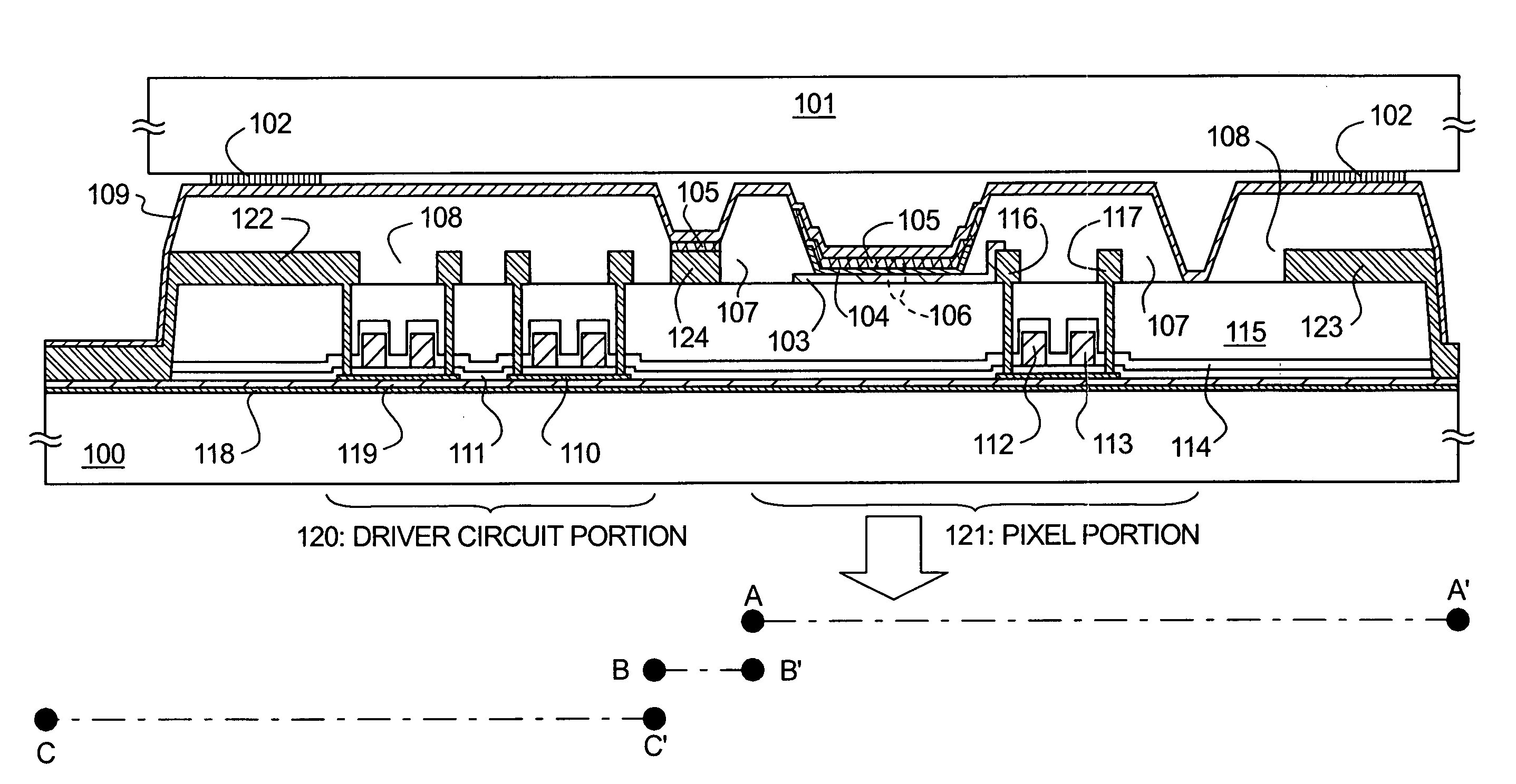
[0052]A first embodiment mode of the present invention will be described with reference to FIG. 1. FIG. 1 is a cross-sectional view showing an active-matrix display device using an organic light-emitting element. The components constituting the display device shown in FIG. 1 will be described in the order of formation.

[0053]A driving circuit portion 120 and a pixel portion 121 are formed by using TFTs on a first substrate 100. As the first substrate 100, a substrate made of glass such as barium borosilicate glass, alumino borosilicate glass, or quartz glass is used.

[0054]The TFT in the driving circuit portion 120 and the TFT in the pixel portion 121 are provided on base films 118 and 119 having insulation properties. A silicon nitride oxide film having a thickness of 10 to 100 nm is formed as the base film 118, whereas a silicon nitride oxide film having a thickness of 20 to 200 nm is formed as the base film 119. In this embodiment mode, silicon nitride oxide film...

embodiment mode 2

(Embodiment Mode 2)

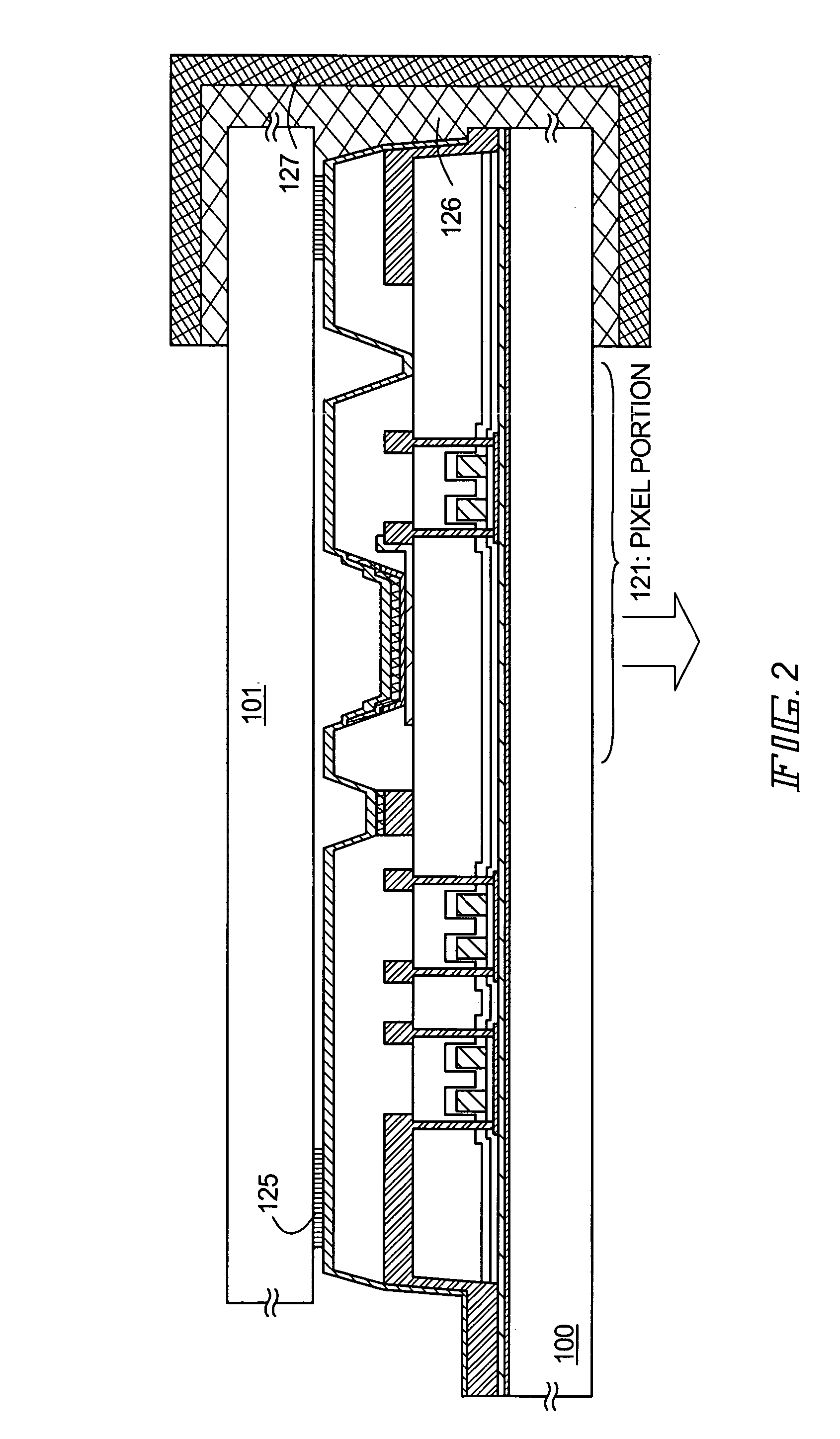
[0076]Embodiment Mode 2 will be described with reference to a cross-sectional view of FIG. 2. FIG. 2 is a cross-sectional view showing an active-matrix organic light-emitting element of Embodiment Mode 2. In Embodiment Mode 2, the display device described in Embodiment Mode 1, whose periphery is further covered with an adhesive and a metal plate 127 having a U-shaped cross section so as to prevent water from entering the organic light-emitting element, is described.

[0077]With the reference to the top plan view of FIG. 6, the adhesive and the metal plate 127 are placed so as not to overlap the pixel portion 121. In the region where the external input terminal 122 is formed so as to attach the FPC 200 thereto, the side face of the first substrate 100 and the side face of the second substrate 101 are separate from each other by 5 to 20 mm. Therefore, the adhesive and the metal plate 127 are provided in the periphery of the region where the end of the first substrate ...

embodiment mode 3

(Embodiment Mode 3)

[0081]Embodiment Mode 3 will be described with reference to a cross-sectional view of FIG. 3. FIG. 3 is a cross-sectional view showing an active-matrix organic light-emitting element according to Embodiment Mode 3. The differences from Embodiment Mode 1 will be described.

[0082]The thicknesses and the materials of the base films, the semiconductor film, the gate insulating film, the gate electrodes, and the first interlayer insulating film are the same as those in Embodiment Mode 1.

[0083]In Embodiment Mode 3, the second interlayer insulating film 115 formed of an organic resin film is thermally cured at 200 to 300° C. A resist is formed on the upper face of the second interlayer insulating film 115, and is then etched by using a reactive gas. After formation of a contact hole reaching the semiconductor film 110, the resist is removed. The surface of the second interlayer insulating film 115 is treated with a plasma using argon or nitrogen as a reactive gas. The rea...


PUM


Abstract

The object of the present invention is to propose a structure of a display device in which water is prevented from passing through the side faces of a display device using an organic light-emitting element and a gap between substrates is made uniform. On the first substrate having the light-emitting element provided thereon, the thicknesses of the layers deposited in the peripheral area, the pixel portion and the driving circuit portion are equalized with each other. Furthermore, an adhesive is provided as thin as possible in the peripheral area of the first substrate so as to bond a second substrate to the first substrate. As a result, the distance between the first substrate and the second substrate can be made uniform throughout the peripheral area of the first substrate, the pixel portion and the driving circuit. Moreover, since a protective film overlying the organic light-emitting element is also provided on the side faces of the second insulating film, water is prevented from entering the display device through its side faces.

Description

BACKGROUND OF THE INVENTION[0001]1. Field of the Invention[0002]The present invention relates to a display device using an organic light-emitting element and a manufacturing method thereof. More specifically, the present invention relates to a sealing structure for protecting an organic light emitting element deposited onto a substrate, and to a display device, in which an element substrate (a substrate having at least an element such as a TFT) and a sealing substrate are provided in the proximity, and a manufacturing method thereof.[0003]Throughout the specification, the term “organic light-emitting element” indicates an element including an organic compound film sandwiched between two electrodes to achieve light emission. One of the representative organic light-emitting elements is a light-emitting element using an organic light-emitting diode (OLED). The OLED includes an organic compound film sandwiched between two electrodes. Holes are injected to one of the electrodes while ele...

Claims


Application Information

Patent Timeline
Patent Type & Authority Patents(United States)
IPC IPC(8): H05B33/00H01L27/32H01L51/52H01L51/56
CPCH01L27/3246H01L51/5246H01L51/525H01L51/5253H01L2251/558H01L51/56H01L2251/5315H10K59/122H10K50/8426H10K50/8428H10K50/844H10K71/00H10K2102/3026H10K2102/351
Inventor YAMAZAKI, SHUNPEIKOYAMA, JUNNISHI, TAKESHISATAKE, RUMO
Owner SEMICON ENERGY LAB CO LTD
Why Eureka
Try Eureka