

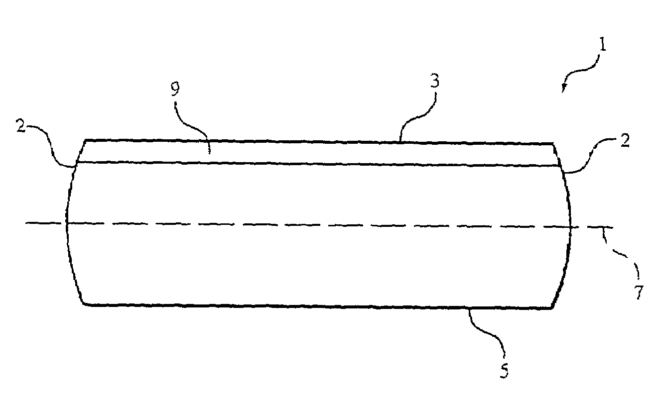
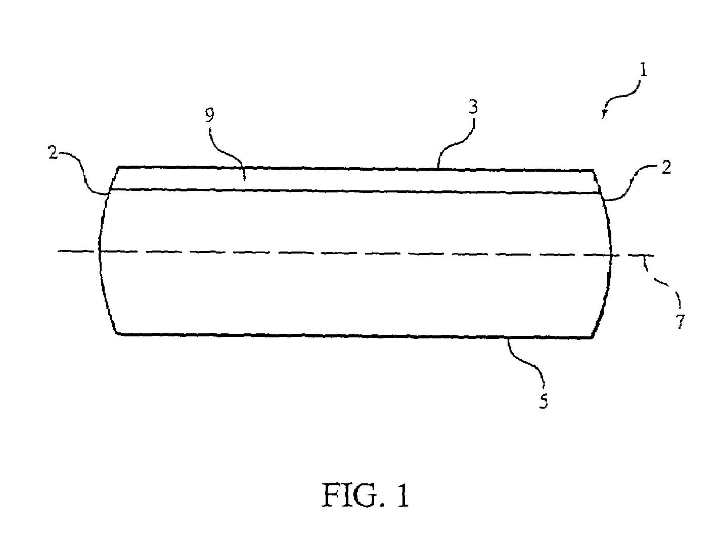
Epitaxially coated semiconductor wafer and process for producing it
a technology of semiconductor wafers and semiconductor wafers, which is applied in the direction of crystal growth process, after-treatment details, polycrystalline material growth, etc., can solve the problems of failure of components, increased failure of components produced on these wafers, and failure of semiconductor wafer production costs with each additional step, so as to improve process reliability, excellent wafer geometry, and reduce the risk of fracture
- Summary
- Abstract
- Description
- Claims
- Application Information
AI Technical Summary
Benefits of technology
Problems solved by technology
Method used
Image

Examples
invention
EXAMPLE (INVENTION)
[0044]300 mm silicon wafers with double-side polished surface, which had been polished and cleaned as described in steps (a) and (b), were available for this example. The roughness of the prepolished wafer was 0.7 nm RMS (AFM, 1 μm×1 μm).
[0045]Step (c): the front surface of the semiconductor wafers was then subjected to a pretreatment prior to the epitaxial coating in the epitaxy reactor, with the aim of, in a first step, removing the native oxide on the front surface and, in a second step, drastically reducing the roughness on the surface, so that after epitaxial coating a semiconductor wafer with considerably improved properties in terms of surface roughness and number of localized light scatterers is available. This was achieved by the fact that, firstly, the native oxide was removed in a hydrogen atmosphere at 1120 degrees Celsius for one minute. Then, gaseous HCl was added to the hydrogen atmosphere for one minute at a temperature of 1140 degrees Celsius, wit...
PUM
| Property | Measurement | Unit |
|---|---|---|
| temperature | aaaaa | aaaaa |
| temperature | aaaaa | aaaaa |
| temperature | aaaaa | aaaaa |
Abstract
Description
Claims
Application Information