Electron beam apparatus and device manufacturing method using same

a technology of chromatic aberration coefficient and device, applied in the direction of beam/ray deflecting arrangement, heat measurement, particle separator tubes, etc., can solve the problems of large aberration coefficient of object lens, unsolved, complex overall apparatus, etc., and achieve the reduction of axial chromatic aberration coefficient, simple structure, and performed in an extremely short time

Inactive Publication Date: 2006-02-14
EBARA CORP
View PDF24 Cites 10 Cited by
  • Summary
  • Abstract
  • Description
  • Claims
  • Application Information

AI Technical Summary

Benefits of technology

[0029]The electron beam apparatus according to the first aspect of the present invention provides advantageous effects represented by the followings.
[0030](1) The dimensions of the electrodes of the objective lens can be designed to provide a filtering effect for secondary electron beams and the axial chromatic aberration coefficient can be reduced.
[0031](2) The throughput is not affected by registration because the registration can be performed in an extremely short time and even during an evaluation on a wafer.
[0032](3) The ExB separator can be implemented for separating secondary electron beams from the primary optical system in a simple structure, and the aberration of the primary electron beam can be readily calculated.
[0033](4) The shot noise can be reduced to 13% of a TFE electron gun.
[0034](5) Even a convexly distored wafer can be flatly chucked.

Problems solved by technology

Particularly, electron beams are widely used in a method of detecting defects of a sample by applying a charge to patterns on the sample, and measuring a resulting potential on the surface for the evaluation because such an evaluation cannot be performed on an optical basis.
When the function of energy filter is given to an objective lens, a problem arises in that the resulting objective lens has a large aberration coefficient.
Also, for correctly aligning a site of a sample under evaluation to the field of view of an electro-optical system, a sub-system is required for registration similar to a lithography system, giving rise to an additional problem that the overall apparatus is increased in size and complicated.
Additionally, in the conventional electron beam apparatus, a variety of problems have been left unsolved, for example, as follows:
(1) In regard to an ExB separator for separating a primary electron beam from a secondary electron beam, it is unknown how a desired accuracy is provided in a simple structure.
(5) The conventional electron beam apparatus experiences difficulties in ensuring a space near a lens located above an objective lens for disposing a deflector for scanning.

Method used


Image

  • Electron beam apparatus and device manufacturing method using same
  • Electron beam apparatus and device manufacturing method using same
  • Electron beam apparatus and device manufacturing method using same

Examples


first embodiment

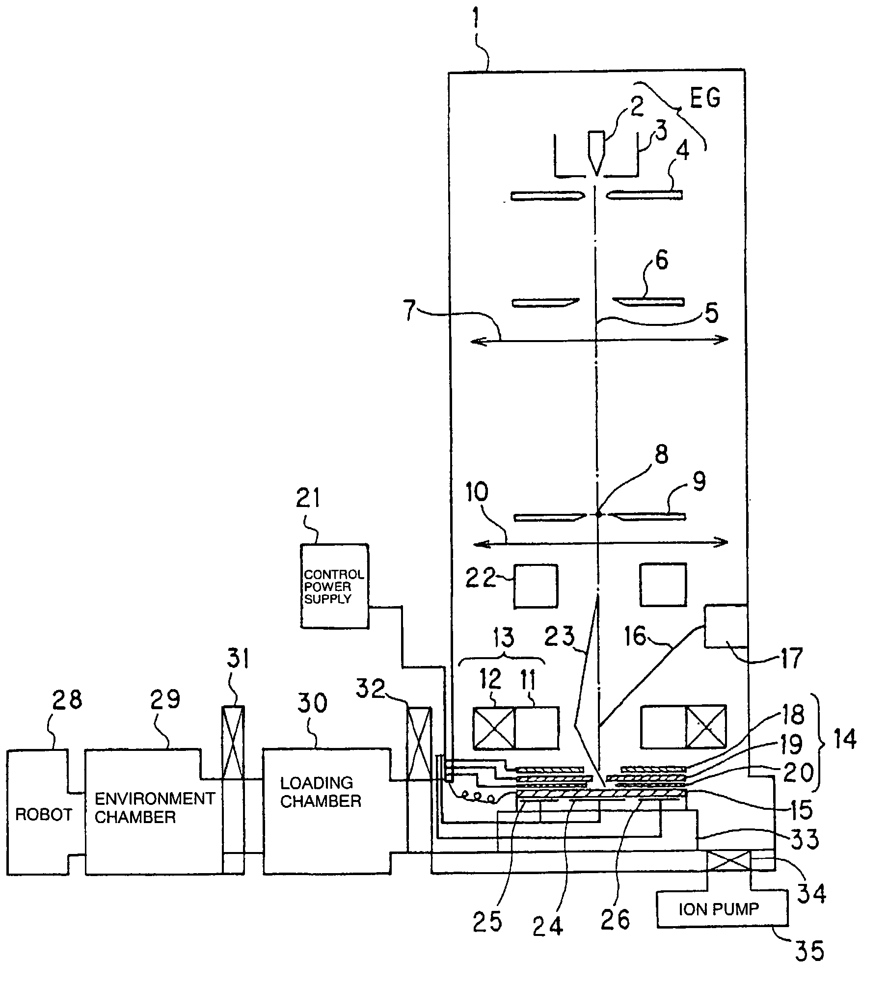
[0064]FIG. 1 generally illustrates an electron beam apparatus according to the present invention. In FIG. 1, an electron-optical column 1 contains an electron gun EG comprised of a cathode 2, a Wehnelt 3, and an anode 4. A primary electron beam emitted from the electron gun EG is irradiated to a first aperture plate 6 having an aperture formed in square on condition that a cross-over 5 is created between the first aperture plate 6 and a first condenser lens 7. In this manner, the primary electron beam that has passed through shaping aperture plate 6 is reduced by the first condenser lens 7 to form a cross-over image 8 on a circular aperture of a second aperture plate 9. The primary electron beam is further reduced by a second condenser lens 10, and passes through an ExB separator 13 made up of an electrostatic deflector 11 and an electromagnetic deflector 12. Then, the primary electron beam is converged by an objective lens 14, and a reduced image of the square aperture formed throu...

second embodiment

[0089]Next, the electron beam apparatus according to the present invention will be described with reference to FIGS. 6 and 7. As illustrated in FIG. 6, the electron beam has a plurality (eight in the illustrated example) of electron-optical columns 100 identical in configuration, arranged side by side on a sample 82. One 101 of the electron-optical columns comprises an electron gun 110; alignment deflectors 74, 75 for aligning a primary electron beam; a condenser lens 76; an electrostatic deflector 77 for scanning the primary electron beam; an ExB separator 111 comprised of an electromagnetic deflector 79 and an electrostatic deflector 80; an objective lens 81; and detector 78 in a detection system for detecting a signal indicative of any of detected secondary electrons emitted from the sample 82, reflected electrons, or absorbed electrons.

[0090]The electron gun 110, which comprises a Wehnelt 72, a thermal electron emitting cathode 71, and an anode 73, emits the primary electron bea...

third embodiment

[0101]Next, the electron beam apparatus according to the present invention will be described with reference to FIGS. 8 and 9. As illustrated in FIG. 8, the electron beam apparatus comprises an electron gun 170; alignment deflectors 144, 145 for aligning a primary electron beam; a condenser lens 146; an aperture 147 formed through a plate in a square shape; an NA aperture 159; a condenser lens 149; alignment deflectors 148, 160 for aligning the NA aperture 159 with condenser lens 149; an electrostatic deflector 150 for scanning the primary electron beam; an ExB separator 153 comprised of an electrostatic deflector 151 and an electromagnetic deflector 152; an objective lens 180 comprised of an upper electrode 154, a central electrode 155, and a lower electrode 156; and a secondary electron detector158 in a detection system for detecting a signal indicative of detected secondary electrons emitted from a sample 157.

[0102]The electron gun 170, which mainly comprises a thermal electron em...


PUM

PropertyMeasurementUnit
thicknessaaaaaaaaaa
voltageaaaaaaaaaa
voltageaaaaaaaaaa

Abstract

An electron beam apparatus is provided for reliably measuring a potential contrast and the like at a high throughput in a simple structure. The electron beam apparatus for irradiating a sample, such as a wafer, formed with a pattern with an electron beam to evaluate the sample comprises an electron-optical column for accommodating an electron beam source, an objective lens, an ExB separator, and a secondary electron beam detector; a stage for holding the sample, and relatively moving the sample with respect to the electron-optical column; a working chamber for accommodating the stage and capable of controlling the interior thereof in a vacuum atmosphere; a loader for supplying a sample to the stage; a voltage applying mechanism for applying a voltage to the sample, and capable of applying at least two voltages to a lower electrode of the objective lens; and an alignment mechanism for measuring a direction in which dies are arranged on the sample. When the sample is evaluated, a direction in which the stage is moved is corrected to align with the direction in which the dies are arranged.

Description

BACKGROUND OF THE INVENTION[0001]The present invention relates to an electron beam apparatus for use with a wafer having patterns with a minimum line width of 0.1 micron or less for evaluating the wafer in a defect test, a line width measurement, an alignment accuracy measurement, and the like, and to a method of manufacturing devices with a high yield rate using the electron beam apparatus.[0002]Conventionally, a defect detection, a CD measurement, a defect review, SEM, an alignment accuracy measurement, and the like have been conducted by known apparatuses which irradiate a sample such as a wafer with an electron beam to detect secondary electrons generated from the sample. Particularly, electron beams are widely used in a method of detecting defects of a sample by applying a charge to patterns on the sample, and measuring a resulting potential on the surface for the evaluation because such an evaluation cannot be performed on an optical basis.[0003]For generating a potential cont...

Claims


Application Information

Patent Timeline
Patent Type & Authority Patents(United States)
IPC IPC(8): G01N23/00H01L21/66G01N23/225H01L21/00
CPCB82Y10/00G01N23/225H01J37/242H01J37/28H01J37/265G01R31/307H01J2237/2817H01J2237/221H01J2237/24507
Inventor NAKASUJI, MAMORUKATO, TAKAOWATANABE, KENJIYOSHIKAWA, SHOJISATAKE, TOHRUNOJI, NOBUHARU
Owner EBARA CORP
Why Eureka
Try Eureka