Scalable gate and storage dielectric

a dielectric and gate technology, applied in the field of gate and storage dielectric systems, can solve the problems of reducing device reliability, inconsistent device characteristics, undesirable charge accumulation at the interface, etc., and achieves the effects of increasing storage capacity, high effective k values, and improving device characteristics

Inactive Publication Date: 2006-02-14
MICRON TECH INC
View PDF19 Cites 25 Cited by
  • Summary
  • Abstract
  • Description
  • Claims
  • Application Information

AI Technical Summary

Benefits of technology

[0018]Gate and storage dielectric systems of the present invention provide high effective K values. Improved gate and storage dielectric stacks include a high K dielectric material that produces improved device characteristics such as increased storage capacity and increased drive current. Additionally, the improved dielectric stacks include a passivated overlayer that maintains the high effective K values, in addition to other desirable characteristics. For example, a silicon-rich-nitride passivated overlayer advantageously provides a stoichiometric interface between a dielectric and a substrate or storage plate. In addition, a silicon-rich-nitride passivated overlayer advantageously provides charge control and regulation of threshold voltage in metal-oxide-semiconductor field effect transistors (MOSFETs).
[0019]Methods of fabricating improved gate and storage dielectric systems are also provided by the present invention. A substrate or bottom storage plate is carefully prepared before subsequent deposition of metal or, in other embodiments, dielectric material. Metal or dielectric materials are deposited to minimize thickness and to maximize storage capacity. Increased storage capacity, which is also characteristic of high K materials, increases area scaling capabilities. Increased area scaling can reduce the integrated circuit chip area required to fabricate an integrated circuit device. Thus, either more devices can be fabricated on a single integrated circuit chip, advantageously allowing increased functionality, or more integrated circuit chips can be fabricated on a single wafer, advantageously reducing costs.
[0020]The passivated overlayer is deposited such that the resulting K value of the overlayer does not compromise the high K value of the dielectric used in the dielectric stack. Dielectric stacks may be appropriately annealed to provide greater stack stability.

Problems solved by technology

Uncontrollable bonding at an interface may decrease device reliability and cause inconsistent device characteristics from one device to another.
Dangling atoms (i.e., atoms that have not formed bonds) from the dielectric material may contribute to an undesirable charge accumulation at the interface.
Charge accumulation varying from device to device can lead to an undesirably varying threshold voltage from device to device.
In addition, leakage characteristics of a dielectric material are particularly important when the dielectric material is used in scaled down devices.
A thin gate dielectric often gives rise to an undesirable tunneling current between a gate and the substrate.
Tunneling current results in wasted power and is particularly destructive in memory circuitry, in which capacitors coupled to a gate dielectric system may be undesirably discharged by the tunneling (i.e., leakage) current.
A gate dopant may undesirably diffuse through a gate dielectric material during high temperature device fabrication, corrupting the substrate / dielectric or plate / dielectric interface.
The dopant may form bonds with the dielectric material and the substrate or plate material causing an undesirable negative charge buildup at the interface.
This negative charge may also result in an undesirable increase in the threshold voltage of the device.
Moreover, the breakdown of a storage dielectric can cause stored charge to undesirably dissipate.
A material that is not significantly etch selective may pose problems in the fabrication of that system or device, as the material may not permit structural integration with other materials of the device.
In an ongoing effort to develop improved dielectric systems, diligent research and experimentation have highlighted problematic dielectric system characteristics.
Attempts to find improved dielectric materials and systems, as defined by the criteria described above, have had limited success.
Particularly, attempts to develop a dielectric system that concurrently satisfies all of the above concerns and issues and that overcomes the limitations of SiO2 have been unsuccessful.

Method used


Image

  • Scalable gate and storage dielectric
  • Scalable gate and storage dielectric
  • Scalable gate and storage dielectric

Examples


Embodiment Construction

[0030]The present invention provides improved dielectric systems and methods of their fabrication in which many quality concerns and issues of dielectric systems are preferably concurrently satisfied.

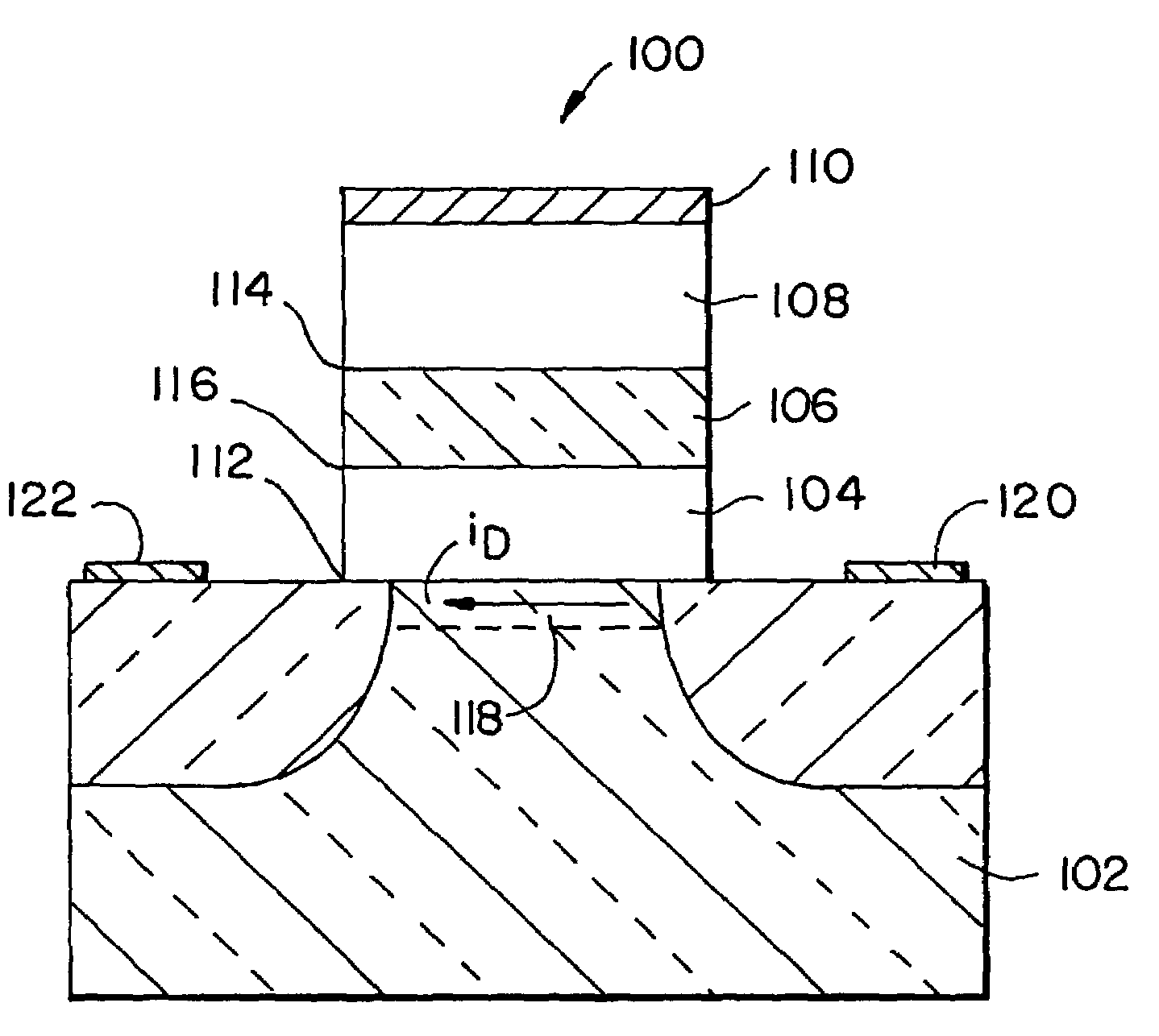
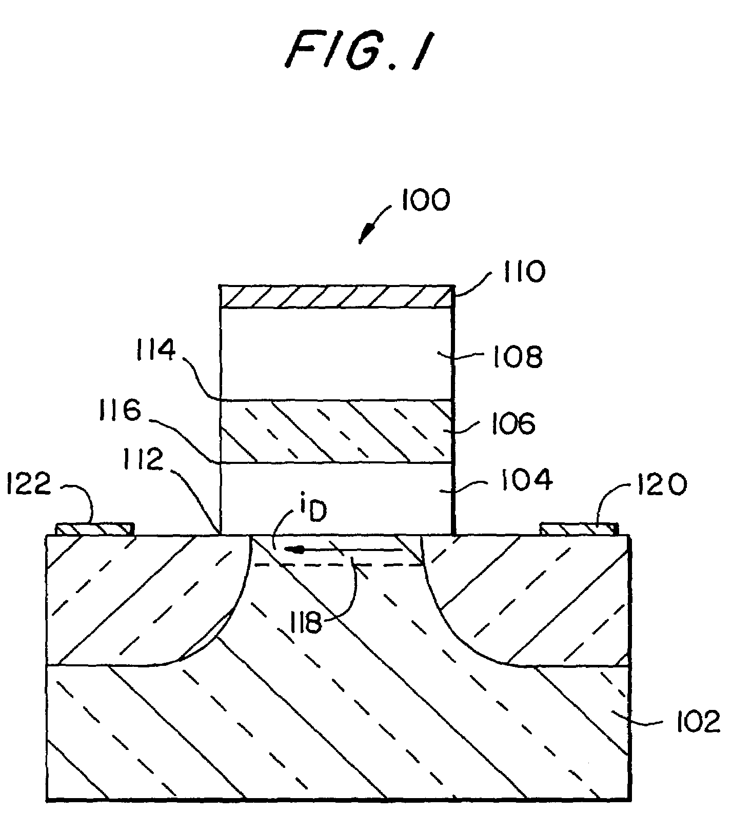
[0031]FIG. 1 shows a gate dielectric stack 100 in accordance with the invention. Stack 100 includes substrate 102, gate dielectric 104, passivated overlayer 106, gate 108, and gate electrode 110. Substrate 102 can be one or more semiconductor layers or structures which can include active or operable portions of semiconductor devices. Generally, substrate 102 comprises silicon (Si). Gate 108 can comprise a degenerate heavily doped polysilicon, a metal, or other conductive material.

[0032]Gate dielectric 104, which can also be referred to as gate insulator 104, includes a single phase stoichiometrically-uniform-composition material having a high dielectric constant (e.g., K≧10) or a silicon or transition-metal doped derivative thereof. A single phase stoichiometrically uniform material inc...


PUM

PropertyMeasurementUnit
refractive indexaaaaaaaaaa
thicknessaaaaaaaaaa
dielectric constantaaaaaaaaaa

Abstract

Gate and storage dielectric systems and methods of their fabrication are presented. A passivated overlayer deposited between a layer of dielectric material and a gate or first storage plate maintains a high K (dielectric constant) value of the dielectric material. The high K dielectric material forms an improved interface with a substrate or second plate. This improves dielectric system reliability and uniformity and permits greater scalability, dielectric interface compatibility, structural stability, charge control, and stoichiometric reproducibility. Furthermore, etch selectivity, low leakage current, uniform dielectric breakdown, and improved high temperature chemical passivity also result.

Description

[0001]This is a divisional of U.S. patent application Ser. No. 10 / 037,081, filed Nov. 9, 2001 now U.S. Pat. No. 6,743,681.BACKGROUND OF THE INVENTION[0002]This invention relates to gate and storage dielectrics of integrated circuit devices. More particularly, this invention relates to scalable gate and storage dielectric systems.[0003]A dielectric is an insulating material capable of storing electric charge and associated energy by means of a shift in the relative positions of internally bound positive and negative charges known as charge dipoles. This shift is brought about by an external electric field. A dielectric system is a collaborating arrangement of materials including at least one dielectric material.[0004]Dielectric systems are directly involved in the progress of microelectronic process technology. Successes in the manufacture of quality dielectric systems have done much to advance integrated circuit technology. Improved dielectric systems have traditionally resulted in ...

Claims


Application Information

Patent Timeline
Patent Type & Authority Patents(United States)
IPC IPC(8): H01L27/108H01L21/02H01L21/28H01L21/334H01L21/336H01L21/8242H01L29/51H01L29/78
CPCH01L21/02049H01L29/78H01L21/02244H01L21/02252H01L21/02362H01L21/28185H01L21/28194H01L21/28202H01L21/28229H01L21/28282H01L21/3143H01L21/3162H01L27/10852H01L27/10861H01L28/55H01L29/513H01L29/517H01L29/518H01L29/66181H01L21/02178H01L21/3141H01L21/31641H01L21/31645H01L27/10811H01L28/40H01L29/40117H10B12/312H10B12/033H10B12/038
Inventor BHATTACHARYYA, ARUP
Owner MICRON TECH INC
Why Eureka
Try Eureka