

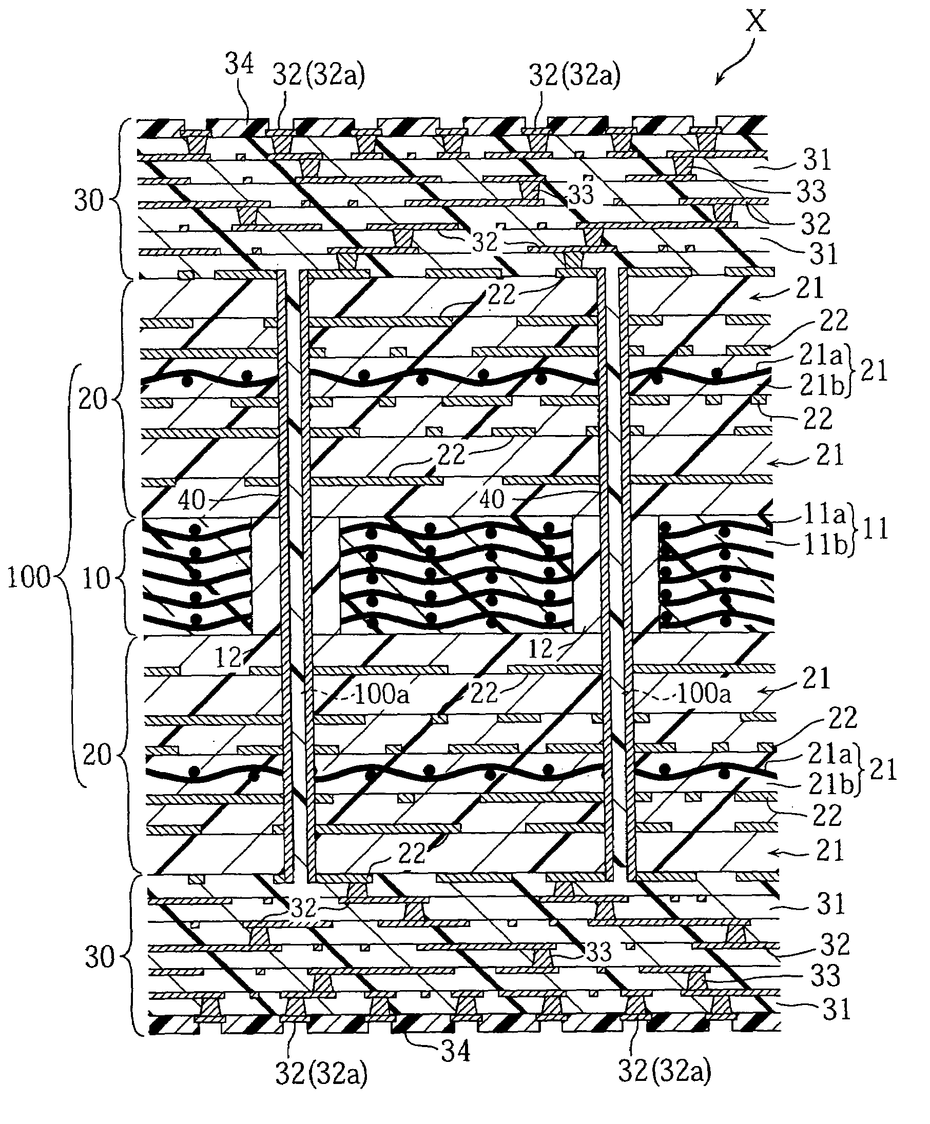
Multilayer wiring board
a multi-layer wiring board and wiring board technology, applied in the direction of printed element electric connection formation, semiconductor/solid-state device details, semiconductor chip details, etc., can solve the problems of easy cracking or separation, electrical connection, and inability to reliably connect wiring boards to semiconductor chips, so as to reduce the overall thermal expansion coefficient of reduce the thermal expansion coefficient of the core portion and therefore of the entire multi-layer wiring board
- Summary
- Abstract
- Description
- Claims
- Application Information
AI Technical Summary
Benefits of technology
Problems solved by technology
Method used
Image

Examples
example 1
[0064]
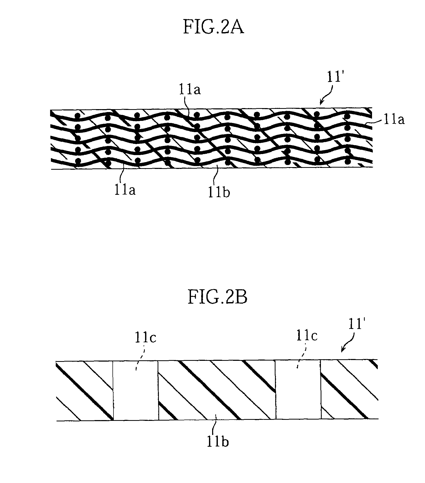
[0065]In this example, the CFRP material was provided by a composite material made from carbon fiber cloth and polyimide resin. The CFRP plate was made as follows: First, a carbon fiber cloth (Brand name: TORAYCA manufactured by Toray Industries Inc.) was impregnated with a modified-polyimide thermosetting resin vanish (a vanish containing monomers and so on which are to be polymerized into polyimide), and then dried to obtain a prepreg having a thickness of 0.2 mm. The carbon fiber cloth was a flat-woven cloth. The cloth was woven of carbon fiber threads made by bundling an average of not less than 200 carbon fibers each having a diameter not greater than 10 μm. In this way, a total of six prepregs were made, then laminated and pressed under vacuum at 200° C. for an hour in the direction of the lamination, to obtain a material CFRP plate having a thickness of 1.2 mm. The CFRP plate had an average thermal expansion coefficient of 0.5 ppm / K along the plane of surface below 150°...
example 2
[0074]
[0075]In this example, the CFRP material was provided by a composite material made from carbon fiber cloth and epoxy resin. The CFRP plate was made as follows: First, a carbon fiber cloth (Brand name: TORAYCA manufactured by Toray Industries Inc.) was impregnated with an epoxy resin vanish (a vanish containing monomers and so on which are to be polymerized into epoxy resin), and then dried to obtain a prepreg having a thickness of 0.2 mm. The carbon fiber cloth was a flat-woven cloth. The cloth was woven of carbon fiber threads made by bundling an average of not less than 200 carbon fibers each having a diameter not greater than 10 μm. In this way, ten prepregs were made, then laminated and pressed under vacuum at 170° C. for an hour in the direction of the lamination, to obtain a material CFRP plate having a thickness of about 2 mm. The CFRP plate had an average thermal expansion coefficient of 0.3 ppm / K along the plane of surface below 150° C.
[0076]Next, the CFRP plate was f...
PUM
| Property | Measurement | Unit |
|---|---|---|
| vol % | aaaaa | aaaaa |
| thickness | aaaaa | aaaaa |
| diameter | aaaaa | aaaaa |
Abstract
Description
Claims
Application Information