Method and fabricating complementary metal-oxide semiconductor image sensor with reduced etch damage

a technology of complementary metal-oxide semiconductors and image sensors, which is applied in the field of can solve the problems of affecting the performance of the complementary metal-oxide semiconductor image sensors, and still being disadvantageous in the described convention methods, so as to improve the low light level sensitivity, improve the sensitivity, and prevent the effect of device characteristics from being degraded

Active Publication Date: 2006-02-28
INTELLECTUAL VENTURES II
View PDF8 Cites 12 Cited by
  • Summary
  • Abstract
  • Description
  • Claims
  • Application Information

AI Technical Summary

Benefits of technology

[0033]It is, therefore, an object of the present invention to provide a method for fabricating a complementary metal-oxide semiconductor (CMOS) image sensor capable of preventing degradation of device characteristics caused by damages created from an etching process and of improving a low light level sensitivity by increasing charge transfer efficiency.

Problems solved by technology

If the photodiode is damaged by a defect in a substrate and a subsequent etching process, the characteristic of the CMOS image sensor may become severely degraded.
Especially, defects in the substrate and lattice defects created in a boundary between a device isolation layer and an active region become a dark current source which impairs performance of the CMOS image sensor.
Despite of the advantage described in FIGS. 2B and 2C, this described convention method still is disadvantageous.
First, although it is possible to prevent the photodiode from being damaged during the blanket etch-back process for forming the spacer, a portion of the substrate disposed in the photodiode side can be still damaged in the course of patterning the gate electrodes, e.g., the transfer gate.
Second, it is difficult to obtain an intended doping profile even though said another P0-type ion implantation process for securing the charge transfer efficiency is employed.
However, this high doping concentration conversely acts as a potential barrier that decreases efficiency on transferring photo-generated electric charges.
As a result of this high energy level, it is difficult to make a delicate control of the doping profile, and this fact results in further difficulty in securing the desired charge transfer efficiency.
Since the P0-type ion implantation region adjacently located in the transfer gate is formed with a thick thickness, the charge transfer efficiency also decreases, thereby deteriorating a characteristic of a dead zone.

Method used


Image

  • Method and fabricating complementary metal-oxide semiconductor image sensor with reduced etch damage
  • Method and fabricating complementary metal-oxide semiconductor image sensor with reduced etch damage
  • Method and fabricating complementary metal-oxide semiconductor image sensor with reduced etch damage

Examples


Embodiment Construction

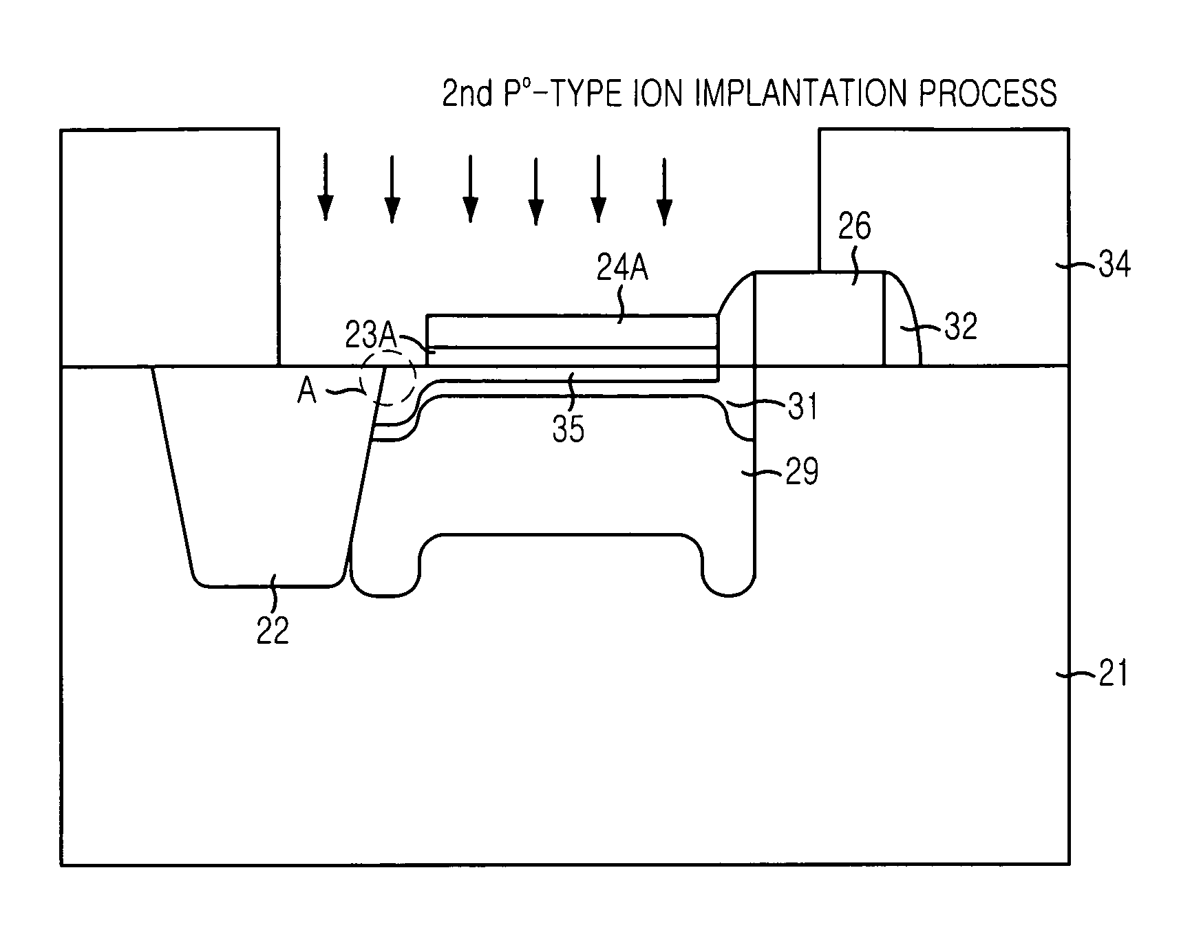
[0045]A method for fabricating a complementary metal-oxide semiconductor (CMOS) image sensor with reduced etch damages in accordance with a preferred embodiment of the present invention will be described in detail with reference to the accompanying drawings, which is set forth hereinafter.

[0046]FIG. 4A is a cross-sectional view showing a substrate structure in a CMOS image sensor in accordance with a preferred embodiment of the present invention.

[0047]As shown, a device isolation layer 22 for defining an active region and a field region is formed in a substrate 21. At this time, it is also possible to use a stacked substrate structure including a substrate with high concentration and an epitaxial layer with low concentration.

[0048]If the above stacked substrate structure, obtained by forming the epitaxial layer with low concentration on the substrate with high concentration, is employed, a depletion layer of a photodiode formed in the epitaxial layer becomes deeper, thereby increasi...


PUM


Abstract

The present invention relates to a method for fabricating a complementary metal-oxide semiconductor (CMOS) image sensor. Prior to forming an N-type ion implantation region and a first and a second P0-type ion implantation regions, an oxide layer and a nitride layer are sequentially formed on a substrate and are subsequently patterned to form a protective pattern structure with a specific arrangement with respect to a photodiode and a gate structure of a transfer transistor. Afterwards, the gate structure is formed on the substrate. In the existence of the protective pattern structure, an N-type ion implantation process for forming the N-type ion implantation region for use in the photodiode, a first P0-type ion implantation process for forming the first P0-type ion implantation region and a spacer formation process are consecutively performed. A second P0-type ion implantation process for forming the second P0-type ion implantation region is performed thereafter.

Description

FIELD OF THE INVENTION[0001]The present invention relates to a complementary metal-oxide semiconductor (CMOS) image sensor; and, more particularly, to a CMOS image sensor with reduced etch damage and improved charge transfer efficiency.DESCRIPTION OF RELATED ARTS[0002]Generally, an image sensor is a semiconductor device that converts an optical image into an electric signal. Charged coupled devices (CCDs) and complementary metal-oxide semiconductor (CMOS) image sensors are representative types of the image sensor.[0003]In the charge coupled device, metal-oxide semiconductor (MOS) capacitors are closely allocated with each other, and charge carriers are transported and stored into the MOS capacitors. Meanwhile, the CMOS image sensor is a device that adopts a switching mode, wherein outputs are sequentially detected by MOS transistors made with the same number of pixels through employing CMOS technology using a control circuit and a signal processing circuit as a peripheral circuit.[0...

Claims


Application Information

Patent Timeline
Patent Type & Authority Patents(United States)
IPC IPC(8): H01L21/00H01L27/146H01L31/10H04N5/335
CPCH01L27/14603H01L27/14689H01L27/14643H01L27/1463H01L27/14609A45D1/04H05B3/20F16J15/3464
Inventor HONG, HEE JEONGLEE, WON-HO
Owner INTELLECTUAL VENTURES II
Why Eureka
Try Eureka