
Backside thinning of image array devices

a technology of image array devices and backside thinning, which is applied in the direction of radiation controlled devices, instruments, optical radiation measurement, etc., can solve the problems of poor resolution, unsuitable non-coplanar surface, and process steps that are not well suited to non-coplanar surfaces, and achieve uniform maximization of pixel fill factor and low resolution , the effect of minimizing electron scattering induced crosstalk

Inactive Publication Date: 2006-02-28
EOTECH LLC
View PDF20 Cites 65 Cited by
  • Summary
  • Abstract
  • Description
  • Claims
  • Application Information

AI Technical Summary

Benefits of technology

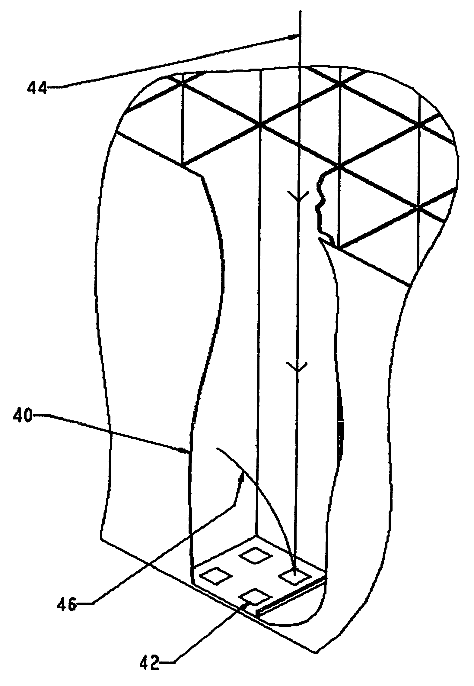
"The patent describes a method for improving the performance of backside thinned image sensors by selectively thinning the backside surface region while leaving the underlying circuitry and bond pads relatively thick. This approach involves using a monolithic collimator structure or a multiple stop layer structure to prevent electron scattering and improve thinning yield. The method also includes a doping ramp to enhance conduction band electrons and improve collection efficiency. Overall, the patent provides a solution for improving the performance and yield of backside thinned image sensors."

Problems solved by technology

This approach replaces metal shield patterning photolithographic process steps, which are not well suited to non-coplanar surfaces such as those generated by ASBT.
Secondary / backscattered electrons arising from the interaction with the anode of the (primary) proximity focused photoelectrons would ordinarily be accelerated along trajectories back to the pixel array, contributing signal to pixels other than that pixel to which the original primary electron was directed, thus contributing to halo, poor resolution, etc.

Method used


Image

  • Backside thinning of image array devices
  • Backside thinning of image array devices
  • Backside thinning of image array devices

Examples


Embodiment Construction

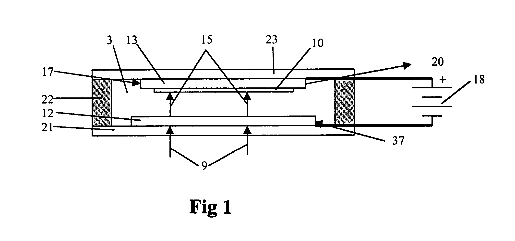
[0028]The context of the invention is illustrated in FIG. 1 where there is shown an example of an electron bombarded active pixel array component including a vacuum enclosure 3 which houses a photocathode 12 such as a GaAs, an InP / InGaAs, a transferred electron photocathode, or a multi-alkali photocathode, in proximity focus with a specialized active pixel array sensor chip 13 which forms the anode for receiving the proximity focused photoelectrons from photocathode 12 to which an acceleration voltage 37 is applied. In accordance with this invention the active pixel array sensor 13 is mounted with its backside 10 facing the photocathode 12. Photoelectrons 15 are emitted from photocathode 12 in response to incident light illustrated as arrows designated 16. Optical components, not shown, are typically employed to form an optical image on the photocathode. Any projection system may be used to place an image on the photocathode.

[0029]The photoelectrons 15 are accelerated by an applied ...


PUM


Abstract

Backthinning in an area selective manner is applied to imaging sensors 12 for use in electron bombarded devices. A further arrangement results in an array of collimators 51 aligned with pixels 42 or groups of pixels providing improved image contrast of such image sensor. Provision of a thin P-doped layer 52 on the illuminated rear surface provides both a diffusion barrier resulting in improved resolution and a functional shield for reference pixels. A gradient in concentration of P-doped layer 52 optimizes electron collection at the pixel array.

Description

RELATED APPLICATIONS[0001]This application is a continuation-in-part of U.S. Ser. No. 10 / 355,838, filed Jan. 31, 2003 now abandoned.FIELD OF THE INVENTION[0002]The invention relates to backthinned and backthinning of solid state imaging sensors.BACKGROUND OF THE INVENTION[0003]Focal plane imaging sensors are well known for the purpose of acquiring an electronic image from a sensor array implemented on a semiconductor die. Particularly widely used such devices include the CMOS imaging array (hereafter, CMOS imager) and the charge coupled device (hereafter, CCD). It is known in prior art to remove material from the backside of substrates, particularly for CCD applications.[0004]Focal plane imaging sensors can be backthinned for a number of reasons. Performance advantages of backthinned sensors can include improved light sensitivity as a result of improved effective fill factor. When properly passivated by a method such as that described in U.S. Pat. No. 5,688,715, backthinned CMOS sen...

Claims


Application Information

Patent Timeline
Patent Type & Authority Patents(United States)
IPC IPC(8): H01L31/00H01LH01L21/00H01L27/146H01L29/04H01L29/06H01L31/062H01L31/113
CPCH01L27/14603H01L27/1464H01L27/14643H01L27/14629H01L27/14625H01L27/14623
Inventor COSTELLO, KENNETH AFAIRBAIRN, KEVIN P.BROWN, DAVID W.CHUNG, YUNGOBER, PATRICIAYIN, EDWARD
Owner EOTECH LLC
Learn More