Parasitic capacitance-preventing dummy solder bump structure and method of making the same

a technology of parasitic capacitance and solder bump, which is applied in the direction of semiconductor devices, semiconductor/solid-state device details, electrical apparatus, etc., can solve the problems of defective electrical performance or even circuit failure of the device, process line width decrease of semiconductor manufacturing, etc., to reduce the electrical performance of the device, and improve the fluidity of the liquid compound in the subsequent packaging process.

Active Publication Date: 2006-04-11
UNITED MICROELECTRONICS CORP
View PDF10 Cites 13 Cited by
  • Summary
  • Abstract
  • Description
  • Claims
  • Application Information

AI Technical Summary

Benefits of technology

[0011]It is an advantage of the present invention against the prior art that the dummy solder bump in the present invention is formed on the UBM layer positioned on the dielectric layer, so that the metal pad between the UBM layer and the dielectric layer according to the prior art is neglected. The parasitic capacitance occurred between the metal pad under the dummy solder bump and the neighboring metal wire as described in the prior art is prevented. Consequently, the fluidity of an underfill liquid compound in subsequent packaging processes is significantly improved without reducing the electrical performance of the device, and the manufacturing yield rate is increased as well.
[0012]These and other objectives of the present invention will no doubt become obvious to those of ordinary skill in the art after reading the following detailed description of the preferred embodiment, which is illustrated in the multiple figures and drawings.

Problems solved by technology

However, as technology progresses, the process line width of semiconductor manufacturing decreases as well.
Parasitic capacitance therefore occurs between the metal pad 24 and the conductive layer 16 due to the shortened distance between the metal pad 24 and the conductive layer as the thickness of the dielectric layer 18 is narrowed, leading to the defective electrical performance or even circuit fail of the device.

Method used


Image

  • Parasitic capacitance-preventing dummy solder bump structure and method of making the same
  • Parasitic capacitance-preventing dummy solder bump structure and method of making the same
  • Parasitic capacitance-preventing dummy solder bump structure and method of making the same

Examples


Embodiment Construction

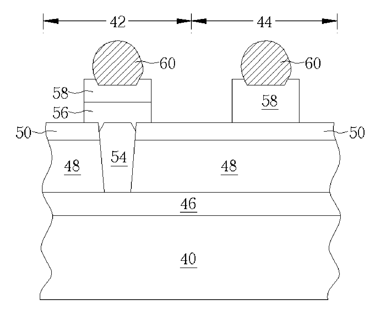
[0015]Please refer to FIG. 5 to FIG. 9 of schematic views of forming a parasitic capacitance-preventing dummy solder bump structure according to the present invention. As shown in FIG. 5, a substrate 40 comprises at least patterned conductive layer 46 positioned on a surface of the substrate 40. The surface of the substrate 40 comprises a first area 42 and a second area 44. Normally, the substrate 40 is a semiconductor wafer with circuits formed inside the semiconductor wafer, and the first area 42 and the second area 44 are respectively a central area and a border area of the surface of the substrate 40.

[0016]As shown in FIG. 6, a chemical vapor deposition (CVD) process is performed to form a dielectric layer 48, comprising either silicon nitride or silicon oxide, on the substrate 40 to cover the conductive layer 46. A passivation layer 50, comprising either silicon nitride or silicon oxide, is formed thereafter on the dielectric layer 48. Alternatively, in another embodiment of th...


PUM

PropertyMeasurementUnit
dielectricaaaaaaaaaa
conductiveaaaaaaaaaa
areaaaaaaaaaaa

Abstract

A parasitic capacitance-preventing dummy solder bump structure on a substrate has at least one conductive layer formed on the substrate, a dielectric layer employed to cover the conductive layer, an under bump metallurgy layer (UBM layer) formed on the dielectric layer, and a solder bump formed on the UBM layer.

Description

BACKGROUND OF INVENTION[0001]1. Field of the Invention[0002]The present invention relates to a method of forming a solder bump structure, and more specifically, to a method of forming a parasitic capacitance-preventing dummy solder bump structure.[0003]2. Description of the Prior Art[0004]High performance microelectronic devices often use solder balls or solder bumps for electrically and mechanically interconnection to other microelectronic devices. For instance, a very large scale integration (VLSI) chip may be electrically connected to a circuit board or other next level packaging substrate by using solder balls or solder bumps. This connection technology is also referred to as “Controlled Collapse Chip Connection (C4)” or “flip chip” technology. The flip chip technology is an area array connection technology and includes reflowing a body of solder onto a bond pad to form a solder bump, so as to electrically connect an IC die to a packaging board.[0005]Please refer to FIG. 1 to FI...

Claims


Application Information

Patent Timeline
Patent Type & Authority Patents(United States)
IPC IPC(8): H01L21/44H01L29/40H01L21/60H01L23/485H01L23/522
CPCH01L24/11H01L24/13H01L23/5222H01L2924/0001H01L2224/131H01L2924/014H01L2224/13099H01L2924/01013H01L2924/01022H01L2924/01029H01L2924/01074H01L2924/01082H01L2924/04941H01L2924/30105H01L2924/01033H01L24/03H01L24/05H01L2224/05001H01L2224/05023H01L2224/05026H01L2224/0508H01L2224/05184H01L2224/05568H01L2224/056H01L2924/00014H01L2224/05124H01L2224/05147H01L2224/05166
Inventor JAO, JUI-MENGSHEU, SHING-RENCHEN, KUO-MINGLIU, HUNG-MINWANG, KUN-CHIH
Owner UNITED MICROELECTRONICS CORP
Why Eureka
Try Eureka