Methods and apparatus for ink delivery to nanolithographic probe systems

a nanolithographic and probe technology, applied in the field of methods and apparatus for ink delivery to nanolithographic probe systems, can solve the problems of inability to achieve advanced ink delivery, inability to use nanolithographic printing ink wells and microfluidics, and many technical challenges

Inactive Publication Date: 2006-04-25
NANOINK INC
View PDF7 Cites 92 Cited by
  • Summary
  • Abstract
  • Description
  • Claims
  • Application Information

AI Technical Summary

Benefits of technology

[0002]Recent advances have been made wherein tips are used to apply inks to surfaces at both the microscopic and nanoscopic scale. For example, tips can be non-hollow and coated with the ink on the tip surface before application of the ink to the surface. Alternatively, tips can be hollow and the ink can pass through the hollow region of the tip to the surface. The result is excellent molecular level control of a printing process. In many cases, the tips or nanoscopic tips and can be used for both ink transfer and for imaging of patterns by scanning probe microscopic methods including atomic force microscopic methods. Physical and chemical interactions between the ink and the surface can be used to engineer the printed structure. Moreover, the meniscus between a nanoscopic tip and the surface can be used to facilitate printing. The processes can be adapted for single tips or multiple tips using single inks or multiple inks. Alignment can be excellent. However, many technical challenges arise with these printing processes at small scale, including the nanoscale, which do not arise with larger scale printing.

Problems solved by technology

However, many technical challenges arise with these printing processes at small scale, including the nanoscale, which do not arise with larger scale printing.
Existing commercial products do not allow for this advanced ink delivery and, generally, little is known about commercial use of ink wells and microfluidics for nanolithographic printing.
Moreover, they are not adapted for use with instruments and printing equipment, particularly at the commercial scale.

Method used


Image

  • Methods and apparatus for ink delivery to nanolithographic probe systems
  • Methods and apparatus for ink delivery to nanolithographic probe systems
  • Methods and apparatus for ink delivery to nanolithographic probe systems

Examples


embodiment 1

A PREFERRED EMBODIMENT 1

Well Plate Interface

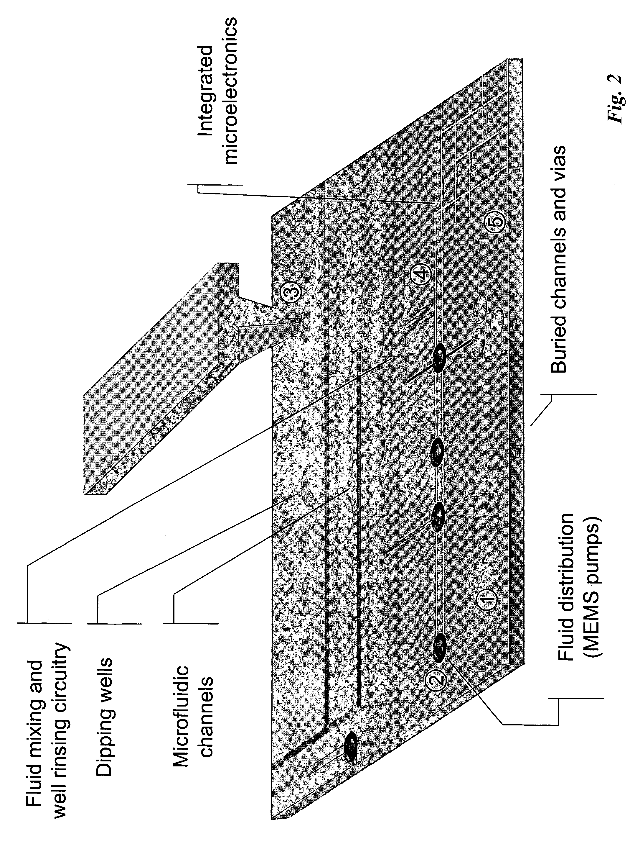
[0231]A preferred embodiment, as illustrated in FIG. 9, includes: a well plate holder and well plate deck 1; a top plate 2; an alignment mechanism 3 that positions the top plate 2 in registry with the well plate underneath. The top plate 2 is equipped with: a fluid aspiration means 4, such as an array of capillaries dipping into the well plate; and microfluidic circuitry 5 that transports the fluids from the capillaries to an ink delivery mechanism 6 (e.g., a microwell array or cantilever array with integrated microfluidics). Fluid transportation may be initiated, e.g., by capillary pumping or by pressurization of the gap between the top plate and the well plate.

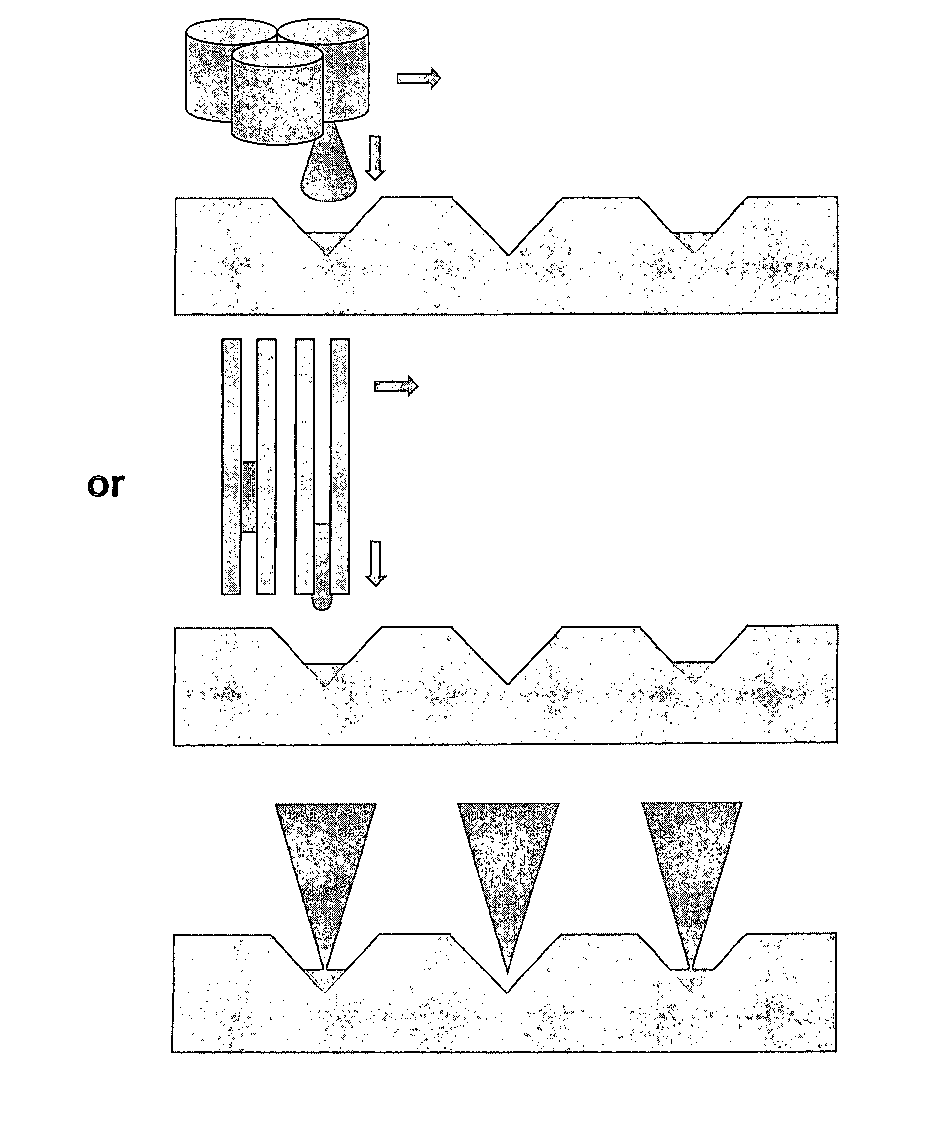
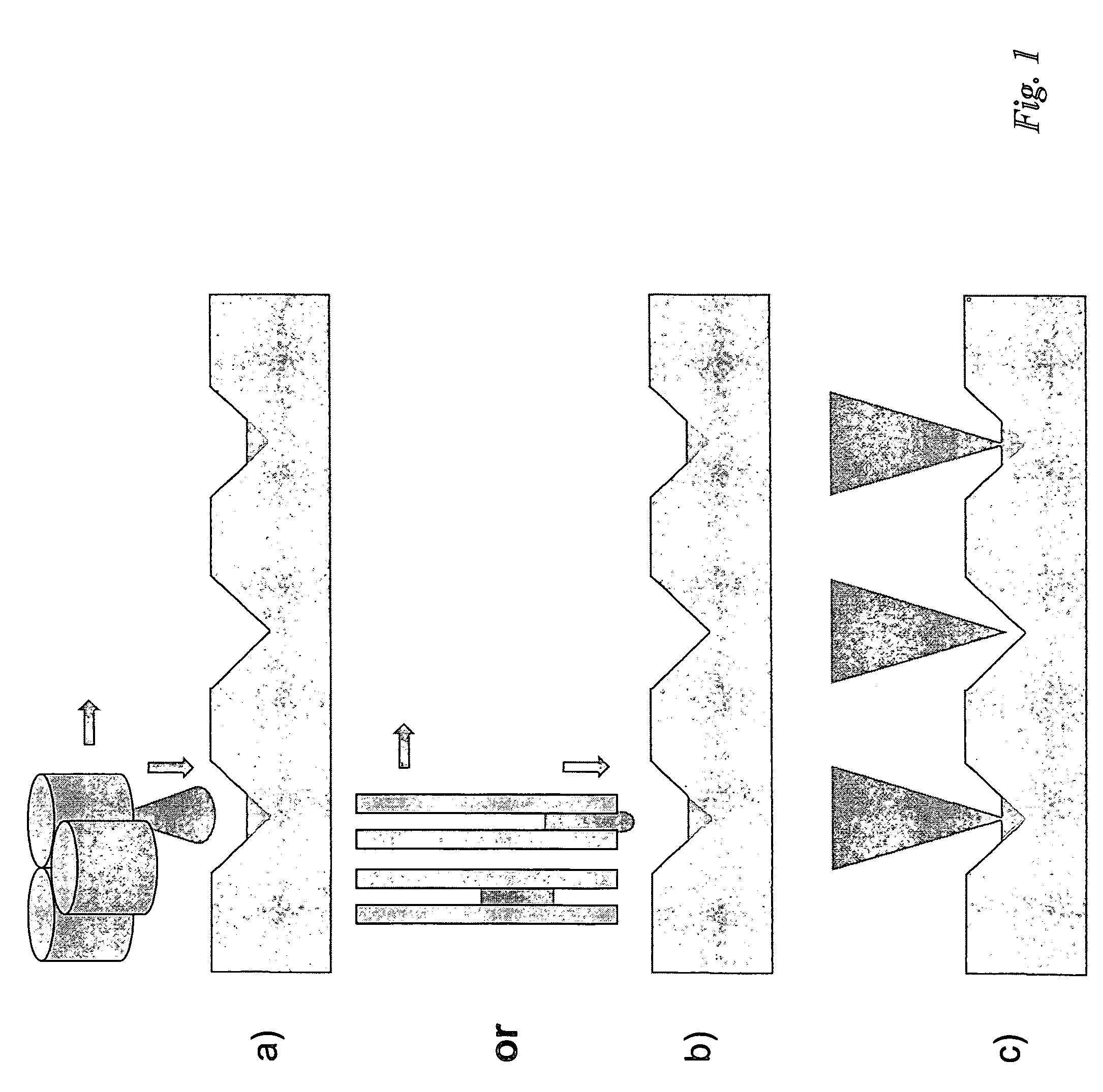
[0232]The well holder could be: (a) a recess with internal dimensions corresponding to the exterior dimensions of the well plate; (b) a set of corners holding the well plate in place; or (c) any other similar device. The well holder is intended to be compatible with commercial plat...

embodiment 2

A PREFERRED EMBODIMENT 2

Delivering Fluid from a Well Plate to an Ink Deposition Means Using Surface Tension Control

[0240]A substrate (e.g., wafer) may be patterned, e.g., using optical lithography or microcontact printing, to expose two or more surface chemistries with differences in their ability to be wet. Examples include, but are not limited to, patterns of thiols or silanes with different ω-functional groups [Kumar, Biebuyck, Whitesides, Langmuir 10 (5): 1498 (1994); Tarlov et al. U.S. Pat. No. 5,514,501 (1996)], the complete disclosures of which are hereby incorporated by reference]. The patterned surface chemistries circumscribe the spreading fluid in contact with the substrate to certain locations on the substrate [Drelich, Miller et al., Colloids and Surfaces 93:1–13 (1994); Gorman, Biebuyck, Whitesides, Chemistry of Materials 7(2):252 (1995), the complete disclosures of which are hereby incorporated by reference], and / or guide the fluids from one location to another, e.g.,...

embodiment 3

Preferred Embodiment 3

Simple Circuit Board-Based Probe Array

[0254]In this embodiment, the probe array is manufactured as a silicon nitride / Pyrex MEMS. The probe array may contain one or more (sealed) ink reservoir(s), from which the ink flow to the probe(s) is electrically controlled, e.g., via a MEMS valving or pumping device. The Pyrex chip is mounted directly on a printed circuit board (PCB). The chip is interconnected to the PCB either by (thermocompression / thermosonic) wire bonding or by flip-chip technology. In the first case, thin gold wires are bound between electrical pads on both the MEMS and the PCB. In the later case, vias are microfabricated in the MEMS main substrate and metallic balls are formed on the backside of the MEMS atop the via openings. The MEMS is soldered in place on matching electrical pads on the PCB or glued with conductive epoxy. The electrical interface between the PCB and the instrument consists of a miniature connector, such as those manufactured by ...


PUM

PropertyMeasurementUnit
contact angleaaaaaaaaaa
apex diameteraaaaaaaaaa
distanceaaaaaaaaaa

Abstract

Inkwells adapted for use in direct-write nanolithography and other applications including use of wells, channels, and posts. The wells can possess a geometry which matches the geometry of tips which are dipped into the inkwells. The channels can be open or closed. Hydrophilicity and hydrophobicity can be used to control ink flow. SEM can be used to characterize the inkwells. Ink flow can be monitored with video. Hydrophobic material layers can be used to prevent cross contamination. Microsyringes can be used to fill reservoirs. Satellite reservoirs can be used to prevent bubble formation.

Description

RELATED APPLICATIONS[0001]This application claims the benefit of provisional application Ser. No. 60 / 425,252 filed Nov. 12, 2002 to Cruchon-Dupeyrat et al. (083847-0188) and Ser. No. 60 / 508,286 to Fragala et al. filed Oct. 6, 2003 (083847-0227); both of these provisional applications are incorporated herein by reference in their entirety including claims and figures.INTRODUCTION[0002]Recent advances have been made wherein tips are used to apply inks to surfaces at both the microscopic and nanoscopic scale. For example, tips can be non-hollow and coated with the ink on the tip surface before application of the ink to the surface. Alternatively, tips can be hollow and the ink can pass through the hollow region of the tip to the surface. The result is excellent molecular level control of a printing process. In many cases, the tips or nanoscopic tips and can be used for both ink transfer and for imaging of patterns by scanning probe microscopic methods including atomic force microscopic...

Claims


Application Information

Patent Timeline
Patent Type & Authority Patents(United States)
IPC IPC(8): B41J2/005B05C1/00B05D5/00B43L25/00G01D15/16G01NG03F7/00
CPCB82Y10/00G03F7/0002B82Y40/00B82Y30/00
Inventor CRUCHON-DUPEYRAT, SYLVAINNELSON, MICHAELELGHANIAN, ROBERTFRAGALA, JOSEPH S.TOUZOV, IGORBANERJEE, DEBJYOTI
Owner NANOINK INC
Why Eureka
Try Eureka