Manufacturing method of semiconductor device

a manufacturing method and semiconductor technology, applied in the direction of semiconductor devices, basic electric elements, electrical equipment, etc., can solve the problems of deterioration of cut-off characteristics, damage to gate insulation film b>6/b>, and difficulty in prolonging the service life of this elemen

Inactive Publication Date: 2006-05-02
DENSO CORP
View PDF21 Cites 65 Cited by
  • Summary
  • Abstract
  • Description
  • Claims
  • Application Information

AI Technical Summary

Benefits of technology

[0025]The present invention is devised to solve the above problems, and has an object to provide a trench gate type semiconductor device having a gate buried in a trench and a manufacturing method of the same, by which it is possible to control variation of a

Problems solved by technology

Accordingly, in the prior art in which the width of the maximum impurity concentration region is narrow, a variation of the threshold value, a destruction of the semiconductor device caused by current concentration due to the variation of the threshold value, and deterioration of cut-off characteristics occur.
In addition, in the case that the semiconductor device having the above-described structure is manufactured as a trench gate type IGBT, there is a technical problem as follows.
Thus, the gate insulation film 6 is damaged by hot carriers due to the concentration of electric field at breakdown.
Hence, there is a technical problem that it is difficult to prolong the service life of this element.
This limiting factor makes it impossible to improve integration.
Hence, the number of steps in the fabrication sequence is increased, whereby the overall cos

Method used


Image

  • Manufacturing method of semiconductor device
  • Manufacturing method of semiconductor device
  • Manufacturing method of semiconductor device

Examples


first embodiment

[0085](First Embodiment)

[0086]Referring to FIG. 1A to FIG. 6, a semiconductor device of the present invention is applied to a MOSFET or an IGBT of a trench gate type.

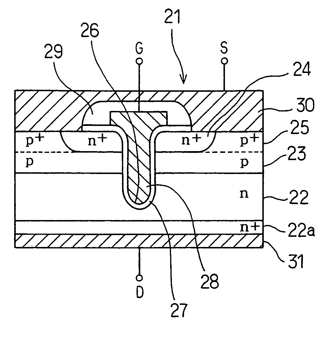
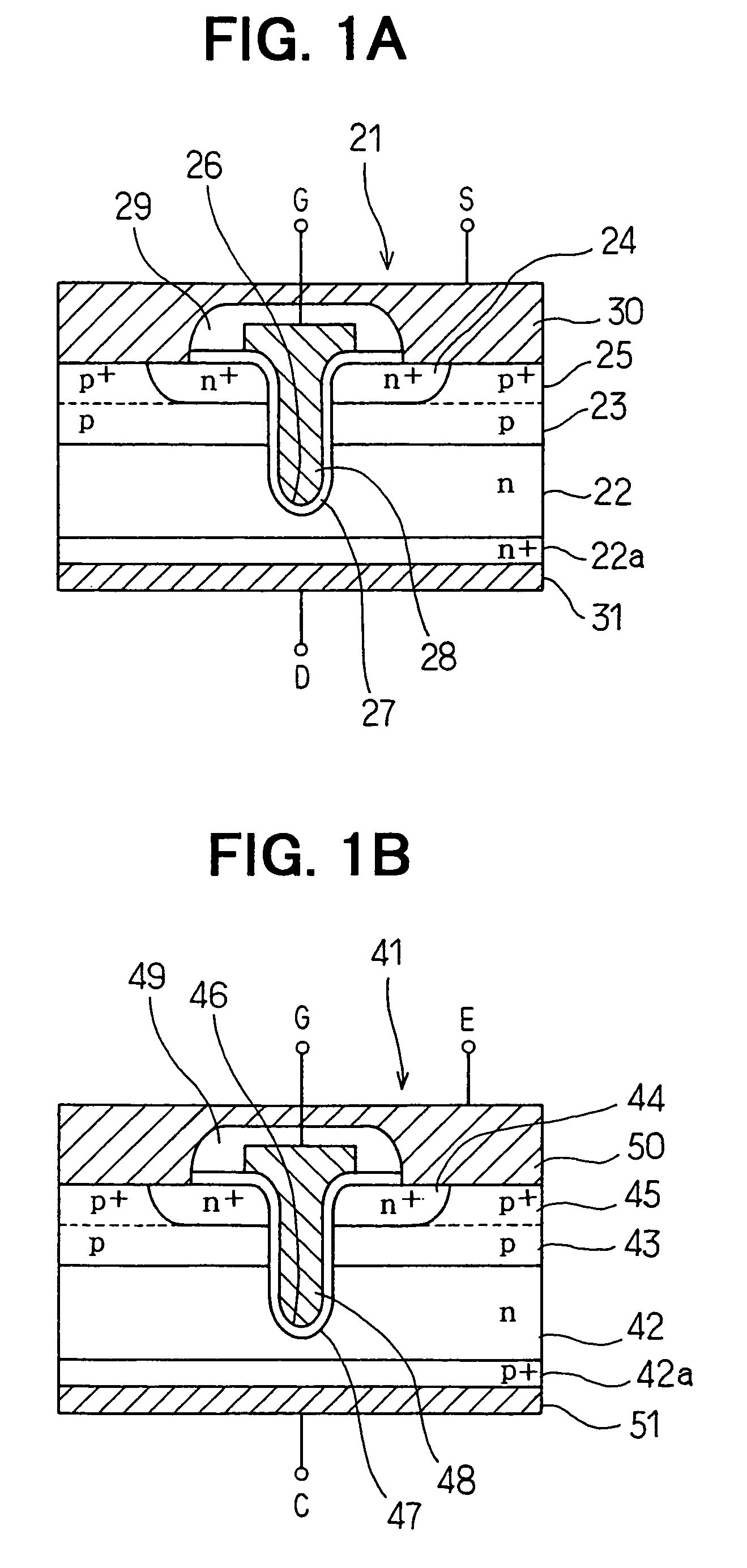
[0087]FIGS. 1A and 1B are cross sections schematically showing structures of a gate portion of a MOSFET 21 and an IGBT 41 adapting the trench gate type structure of the present invention, respectively.

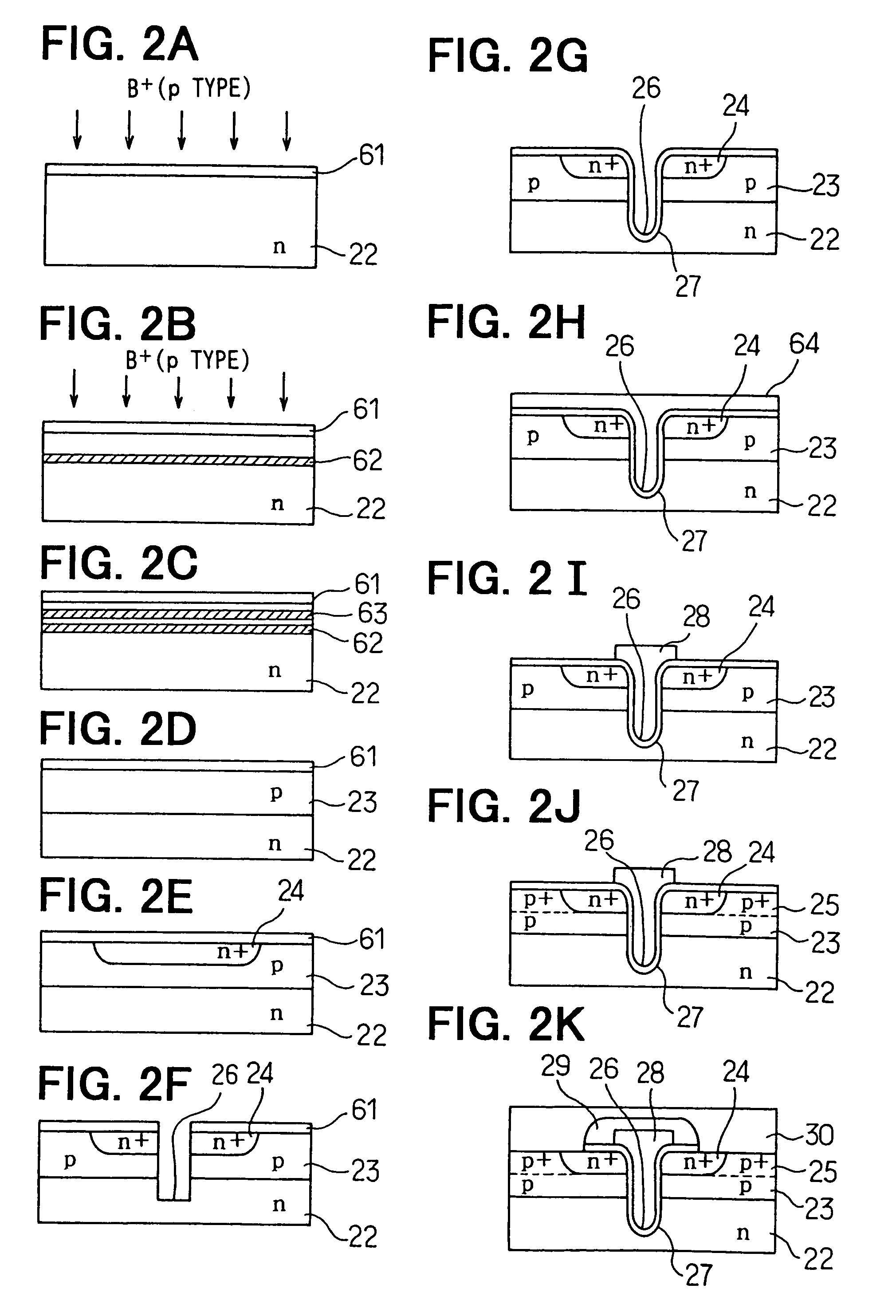
[0088]First of all, the following description will describe the MOSFET 21 with reference to FIG. 1A. A semiconductor substrate 22 having a n-type conductivity defined herein as a first conductivity type is provided with a highly doped n-type region 22a at a back surface thereof. Additionally, an island of a base region 23 is formed on a principal surface of the semiconductor substrate as a second conductivity type region, which is formed by introducing impurities of p-type defined herein as a second conductivity type into a region corresponding to an element forming region with plural of times ion implantations (FIG. 1A sh...

second embodiment

[0108](Second Embodiment)

[0109]The following description will describe a second embodiment of the present invention with reference to FIGS. 7 through 17 chiefly regarding a difference from the first embodiment. The second embodiment includes a first type of the basic arrangement and various modifications. Thus, the structure and manufacturing method of each will be explained first, and thence measured value of electric characteristics for each will be explained.

[0110](1) First Type

[0111]FIG. 7 is a schematic cross section of a trench gate type IGBT 71 of the first type as a basic arrangement. The following description will describe a difference between the IGBT 71 and the IGBT 41 of the first embodiment. The trench gate portion of the IGBT 71 is basically the same as that of the IGBT 41, and additionally, an emitter trench 72 is formed as a second trench in the base region 43 between adjacent trenches 46 each as a first trench, and a P body region 73 as a second conductivity type pr...

third embodiment

[0142](Third Embodiment)

[0143]FIGS. 18 and 19 show a third embodiment of the present invention, which is devised to improve a structure of a peripheral portion to attain a high withstand voltage. The present embodiment is applicable to each type of the second embodiment provided with the P body layer (region) 73, so that no additional step is necessary in the manufacturing sequence to improve the structure of the peripheral portion.

[0144]According to the arrangement herein, as shown in FIG. 18, a guard ring 91 is formed as an electric field alleviating region with a junction deeper than that of the base region 43 in such a manner so as to enclose a peripheral portion of an island of the p-type base region 43. In addition, for example, four field limiting rings 92 each also having a deep junction are provided as four annular electric field alleviating regions in the n-type semiconductor substrate 42 at an outside of the base region 43.

[0145]The number, junction depth, and spacing of ...


PUM


Abstract

By improving profile of impurity concentration in a channel portion of an FET or an IGBT of a trench gate type, variation of threshold value is lessened, and a destruction caused by current concentration is prevented while suppressing deterioration of cut-off characteristics. An island of a base region of p-type is formed in a semiconductor substrate of n-type by carrying out high acceleration ion implantation twice followed by annealing, so that the impurity concentration profile in a channel portion changes gradually in a depth direction. Accordingly, it is possible to lessen variation of the threshold value and to reduce pinch resistance while at the same time improving sub-threshold voltage coefficient and conductance characteristics.

Description

CROSS REFERENCE TO RELATED APPLICATION[0001]This application is a divisional application of U.S. patent application Ser. No. 09 / 865,704 filed May 29, 2001, now abandoned, which is based on Japanese Patent Application No. 2000-159685 filed on May 30, 2000, the contents of which are incorporated herein by reference.BACKGROUND OF THE INVENTION[0002]1. Field of the Invention[0003]The present invention relates to a semiconductor device adapting a trench gate structure (with a gate buried in a trench), and more particularly to a trench gate type semiconductor device capable of withstanding a high voltage and a manufacturing method of the same.[0004]2. Related Arts[0005]With regard to a semiconductor device serving as an integrated circuit, there have been proposed various structures, in one of which, for example, elements are isolated by a trench provided on a surface of a semiconductor substrate as one of trends for improving in degree of integration and for improving characteristics. On...

Claims


Application Information

Patent Timeline
IPC IPC(8): H01L21/336H01L29/06H01L29/10H01L29/739H01L29/78
CPCH01L29/0696H01L29/7813H01L29/1095H01L29/7811H01L29/66734H01L29/41766
Inventor ITO, HIROYASUKATO, MASATOSHIARAKAWA, TAKAFUMI
Owner DENSO CORP
Why Eureka
Try Eureka