Gallium-nitride based multi-quantum well light-emitting diode n-type contact layer structure
a gallium-nitride and multi-quantum well technology, applied in the field of gallium-nitride based multi-quantum well light-emitting diodes, can solve the problems of n-type gan contact layer easily chapped and snapped, affecting the epitaxial quality of gan-based mqw, and excessive stress to develop and accumulate. , to achieve the effect of convenient formation
- Summary
- Abstract
- Description
- Claims
- Application Information
AI Technical Summary
Benefits of technology
Problems solved by technology
Method used
Image
Examples
first embodiment
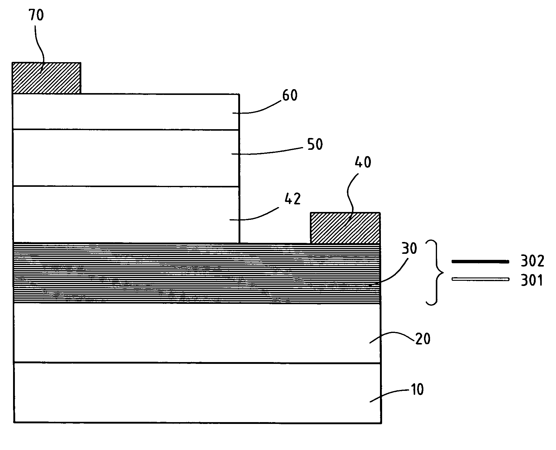
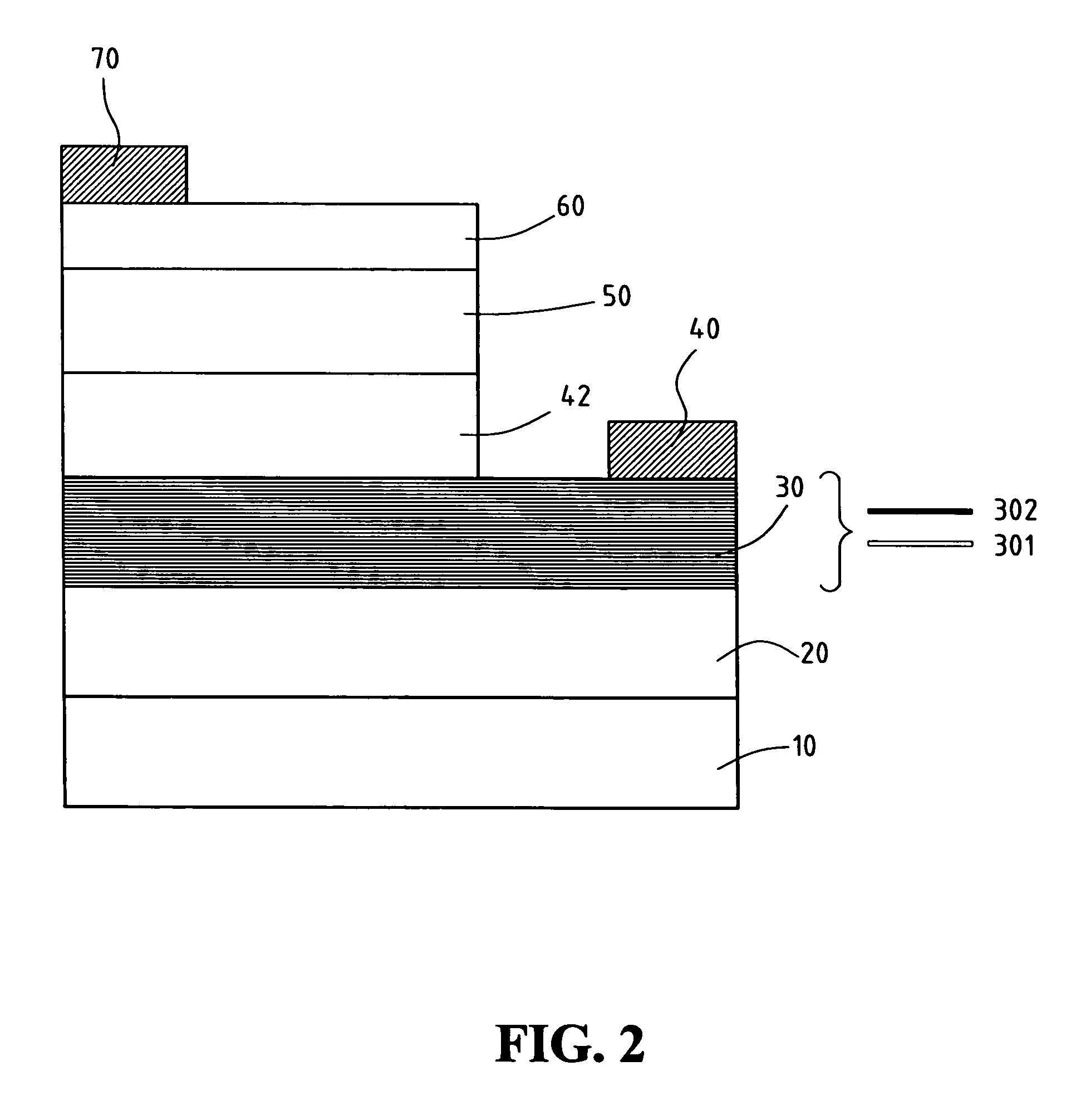
[0018]FIG. 2 is a schematic diagram showing the epitaxial structure of the GaN-based MQW LED according to the present invention. As shown in FIG. 2, the GaN-based LED has a substrate 10 made of C-plane, R-plane, or A-plane aluminum-oxide monocrystalline (sapphire), or an oxide monocrystalline having a lattice constant compatible with that of nitride semiconductors. The substrate 10 can also be made of SiC (6H-SiC or 4H-SiC), Si, ZnO, GaAs, or MgAl2O4. Generally, the most common material used for the substrate 10 is sapphire or SiC. A buffer layer 20 made of AlaGabIn1-a-bN (0≦a,b10. On top of the buffer layer 20, an n-type contact layer 30 is formed, which is the major focus of the present invention. Then, on top of n-type contact layer 30, an active layer 42 made of InGaN covers a part of the n-type contact layer 30's upper surface. A negative electrode 40, on the other hand, is on top of another part of the n-type contact layer 30's upper surface not covered by the active layer 42....
fourth embodiment
[0023]FIG. 5 is a schematic diagram showing the epitaxial structure of the GaN-based MQW LED according to the present invention. As shown in FIG. 5, the n-type contact layer 36 has a structure identical to those of the n-type contact layers of the previous embodiments. The only difference lies in the materials used for the n-type contact layer 36. Within this embodiment of the present invention, as shown in FIG. 5, the n-type contact layer 36 has a superlattice structure formed by multiple Si-doped AlInGaN base layers 361 and multiple Si-doped AlInGaN base layers 362, alternately stacked on top of each other. Among them, the AlInGaN base layers 362 have wider band gaps than those of the AlInGaN base layers 361. The n-type contact layer 36 can have either an AlInGaN base layer 361 or an AlInGaN base layer 362 as the bottommost base layer. That is, the n-type contact layer 36 can comprise an AlInGaN base layer 361, an AlInGaN base layer 362, another AlInGaN base layer 361, etc., seque...
PUM
 Abstract
Description
Claims
Application Information


