Radial scan arm and collimator for serial processing of semiconductor wafers with ribbon beams

a technology of ribbon beams and scan arms, which is applied in the direction of irradiation devices, electric discharge tubes, electrical apparatus, etc., can solve the problems of contaminating the wafer, difficult lubrication of the moving mechanism in vacuum, and more rapid wear

Active Publication Date: 2006-06-06
ADVANCED ION BEAM TECHNOLOGY INC
View PDF3 Cites 30 Cited by
  • Summary
  • Abstract
  • Description
  • Claims
  • Application Information

AI Technical Summary

Benefits of technology

[0040]A further aspect of the invention is to provide a means of causing the ion beam to vary in current density in proportion to the distance from the scan pivot, thereby allowing a uniform dose of ions to be imparted in spite of the radial variation of the scan velocity. This variation is accomplished by means of a non-linear transfer function in one or more ion optical elements. Such elements may be magnet poles or pole edges, or multipole lenses of various types including magnetic and electrostatic components.
[0042]Yet another aspect of the invention allows the above-described aspects to be utilized in the case where a suitable ribbon-shaped beam is unavailable, and instead, an ion beam of transverse dimensions smaller than the workpiece is available. This aspect provides a sliding seal mechanism with vertical linear bearings and scan actuator mounted in atmosphere, incorporating a plate from which the scan mechanisms described above may be mounted, through a slot in the vacuum wall on a cantilevered member, in such a manner that the entire scan mechanism may be scanned in a vertical direction through a distance exceeding the dimension of the workpiece, effective to scan the workpiece mechanically in a 2D raster pattern through the ion beam, thereby imparting a uniform dose of ions at a specified angle to a surface of the workpiece.

Problems solved by technology

The difficulties in engineering durable equipment for performing single wafer hybrid ion implantation include: (a) the need to minimize the mass of the moving assembly while retaining stiffness; (b) the need to provide a reliable seal between the vacuum in which the process occurs and the atmosphere; (c) the need to provide a means of tilting the wafer with respect to the beam axis; and (d) simultaneously, the need to keep the mechanism simple, reliable, and accessible for service.
However, moving mechanisms in vacuum are difficult to lubricate, and suffer from more rapid wear than those in atmosphere.
Furthermore, lubricants are potential contaminants of the process; and friction in the vacuum will generate particles which can contaminate the wafer.
In addition, air bearings are reliable but expensive.
It is required to have great precision and low backlash.(ii) The motion from the implant location to the load position is a complex long motion requiring modest accelerations to ensure that the wafer is securely retained, thereby limiting overall throughput of the implant system(iii) The load position is not sufficiently remote from the beam and limits the space for instrumentation(iv) The required rotary motion involves active deceleration and acceleration during the passage of the wafer through the beam, in order to accomplish uniform projection of velocity on a straight line.
This unfortunately introduces a high risk of backlash-generated velocity errors.

Method used


Image

  • Radial scan arm and collimator for serial processing of semiconductor wafers with ribbon beams
  • Radial scan arm and collimator for serial processing of semiconductor wafers with ribbon beams
  • Radial scan arm and collimator for serial processing of semiconductor wafers with ribbon beams

Examples


first embodiment

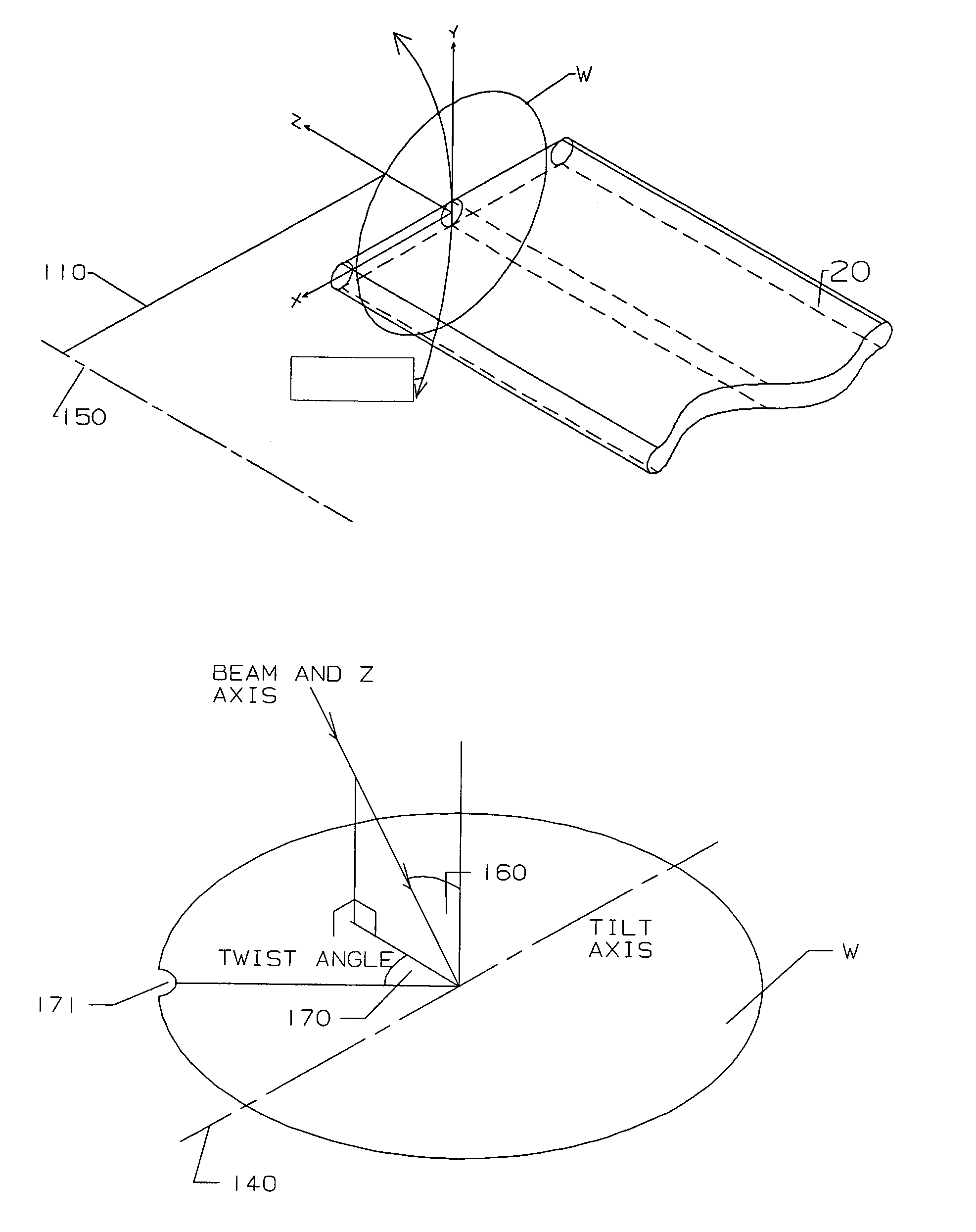
[0098]In the first embodiment illustrated by FIG. 6, the ribbon beam 20 is traveling horizontally and its long dimension is in the horizontal plane. This means that the x and z axes are horizontal and the y-axis is vertical. The workpieces to be implanted are 300 mm silicon wafers. The radial scan arm 110 is 450 mm long, and its pivot lies in the plane y=0. The scan pivot axis is of course aligned with the beam z-axis, and the alignment may be confirmed [by methods described in U.S. patent application Ser. No. 10 / 807,772, filed Mar. 24, 2004, or by other methods].

[0099]The tilt pivot axis 140 lies in a plane inclined to the z-axis, and does not intersect the scan pivot axis. Its orientation is defined as follows: in order for the edge of the wafer to clear the ion beam, the arm must pivot through an angle whose sine exceeds (150 mm / 450 mm), i.e. by + / −19.5 degrees. To allow for the finite y-extent of the beam (probably + / −30 mm) the arm would have to be rotated through an angle of +...

second embodiment

[0108]As shown by FIG. 7, in this second embodiment the ribbon beam is also traveling horizontally, but its long dimension is in the vertical plane. This means that the y and z axes are horizontal, and the x-axis is vertical. The arm is 450 mm long, and its pivot lies in the plane y=0, aligned with the beam z-axis. The tilt pivot axis in this case is aligned with the radial arm. From the mid-point of the wafer scan, the load / unload position is reached by rotating the radial arm by 90 degrees so that its length is parallel to the y-axis, and then rotating 90 degrees about the tilt pivot axis so that the wafer surface is horizontal. These rotations have been defined sequentially, but in practice they occur simultaneously to save time.

[0109]The arm pivot axis may be located either above or below the beam. However, a location above the beam (as shown in FIG. 7) is preferable so that particles generated by the beam, or by surfaces it may strike, are prevented from falling on to the wafer...

third embodiment

[0115]An additional mechanism may be used in conjunction with this or other embodiments of the invention as a means of providing a two-dimensional mechanical scan. To meet this end, this third embodiment may be mounted on a movable slide effective to move the entire radial arm scan assembly in the vertical direction. Accordingly, it may now be used to mechanically scan the wafer in two orthogonal directions; and this is very useful under certain conditions (e.g., very low energies below 1 keV and high currents of several mA) where a sufficiently uniform ribbon beam is hard to obtain. In this case, a beam 21 which is approximately circular or rectangular, as illustrated in FIG. 10, can be used.

[0116]Also, the low energy beam can be manipulated by a multipole lens to reduce its size considerably. FIG. 10 illustrates the structure of this arrangement. As seen therein, the sliding seal may be constructed using nested seals of delrin or similar plastic, with the intervening space differe...


PUM


Abstract

Semiconductor wafers are sequentially mounted on a holder at one end of an arm which is pivoted about its other end. Each wafer is thereby passed on an arcuate path through a parallel-scanned or continuous ribbon-shaped beam for processing. The pivot axis is parallel to the centroid of the beam trajectories. By pre-orienting the wafers before loading, and by providing a second pivot between the arm and the holder, the angle between the beam and the wafer surface may be precisely adjusted to any arbitrary angle of interest. The geometry is such that this angle is constant over the processed area. Uniform processing requires a scanned ribbon beam to have a non-uniform scan velocity and a continuous ribbon beam to have a non-uniform intensity profile. The required non-uniformity is generated by a suitably shaped collimating magnet. When a suitable ribbon beam is unavailable, a beam of approximately circular shape may be used by translating the pivot axis, thereby moving the wafer in a two-dimensional pattern through the beam.

Description

PRIORITY CLAIM[0001]The present invention was first filed as the subject matter of U.S. Provisional Patent Application Ser. No. 60 / 542,570 filed Feb. 6, 2004 and entitled “Radial scan arm and collimator for serial processing of semiconductor wafers-with scanned beams.”FIELD OF THE INVENTION[0002]The present invention applies to the processing of workpieces by ion beams. More particularly, the invention is directed to the ion implantation of workpieces, such as silicon wafers, with parallel continuous ribbon ion beams or scanned ribbon ion beams; and passes the workpiece over an arc-shaped path through the ion beam in a manner that gives greater control of the angle between the ions and the entire implanted surface of the workpiece, and allows for an improved control of the uniformity of the dose.BACKGROUND OF THE INVENTION[0003]Existing equipment and methods for ion implantation process wafers either singly or in batches. Batch processing is usually performed on spinning disks which...

Claims


Application Information

Patent Timeline
Patent Type & Authority Patents(United States)
IPC IPC(8): H01J37/20H01J37/08H01J37/317H01L21/00
CPCH01J37/3171H01L21/67069H01J2237/20228
Inventor KAIM, ROBERT E.WHITE, NICHOLAS R.
Owner ADVANCED ION BEAM TECHNOLOGY INC
Why Eureka
Try Eureka