

Front illuminated back side contact thin wafer detectors
- Summary
- Abstract
- Description
- Claims
- Application Information
AI Technical Summary
Benefits of technology
Problems solved by technology
Method used
Image

Examples
Embodiment Construction
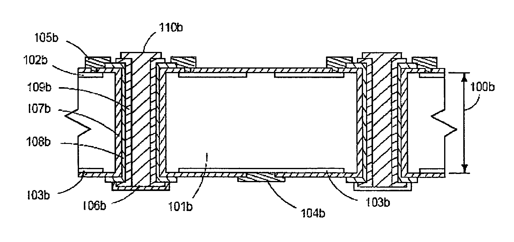
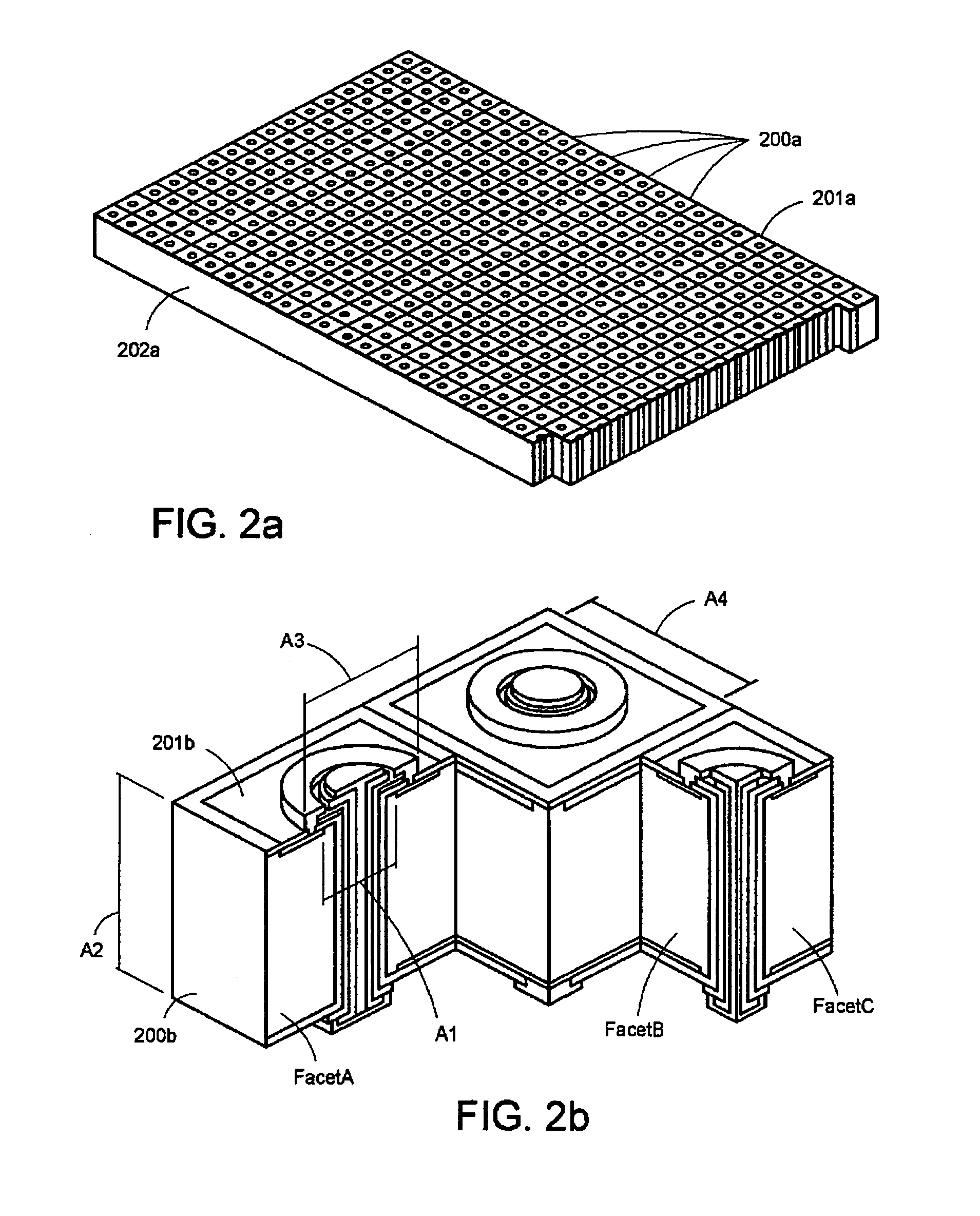
[0037]The present invention is directed toward a detector structure, detector arrays, a method of detecting incident-radiation, and a method of manufacturing the detectors. The present invention comprises several embodiments that provide for reduced radiation damage susceptibility, decreased affects of cross-talk, and increased flexibility in application. Various modifications to the disclosed embodiments will be readily apparent to those of ordinary skill in the art, and the disclosure set forth herein may be applicable to other embodiments and applications without departing from the spirit and scope of the present invention and the claims hereto appended. Thus, the present invention is not intended to be limited to the embodiments described, but is to be accorded the broadest scope consistent with the disclosure set forth herein.
[0038]In one embodiment, the present invention comprises a plurality of front side illuminated photodiodes, optionally organized in the form of an array, ...
PUM
 Abstract
Description
Claims
Application Information