Method of forming capacitor with ruthenium top and bottom electrodes by MOCVD

a top and bottom electrode, ruthenium technology, applied in the direction of solid-state devices, coatings, chemical vapor deposition coatings, etc., can solve the problems of inability to achieve the aspect ratio of one or more three-dimensional devices, poor step coverage of three-dimensional structures, etc., to achieve high integration degree, high aspect ratio, and capacity increase

Inactive Publication Date: 2006-07-04
HITACHI LTD
View PDF12 Cites 1 Cited by
  • Summary
  • Abstract
  • Description
  • Claims
  • Application Information

AI Technical Summary

Benefits of technology

[0006]This invention has been accomplished to overcome the foregoing problems and has the object of providing a semiconductor device, including a dielectric capacitor having excellent step coverage in a device structure at a high aspect ratio, along with a high integration, as well as a manufacturing method of manufacture thereof.
[0027]Further, in accordance with this invention, since the organic ingredient of the precursor and the reaction gas are subjected to combustion or reductive reaction in the course of forming the film when O2, H2, CO or CO2 is used as the reaction gas, the residual carbon content in the electrode film for the bottom electrode and the top electrode can be defined as 10−2 at % or more and 1 at % of less, by which a high quality bottom electrode and top electrode not causing contact failure can be formed, and a semiconductor device with high performance can be manufactured.

Problems solved by technology

In the prior art described above, since Pt or Ru of the bottom electrode is prepared by the sputtering method, there is a problem in that the three-dimensional structure shows poor step coverage, and adhesion to the inside wall is small compared with that to the surface and the bottom, so that a highly three-dimensional device structure with an aspect ratio of one or more can not be attained.

Method used


Image

  • Method of forming capacitor with ruthenium top and bottom electrodes by MOCVD
  • Method of forming capacitor with ruthenium top and bottom electrodes by MOCVD
  • Method of forming capacitor with ruthenium top and bottom electrodes by MOCVD

Examples


example 1

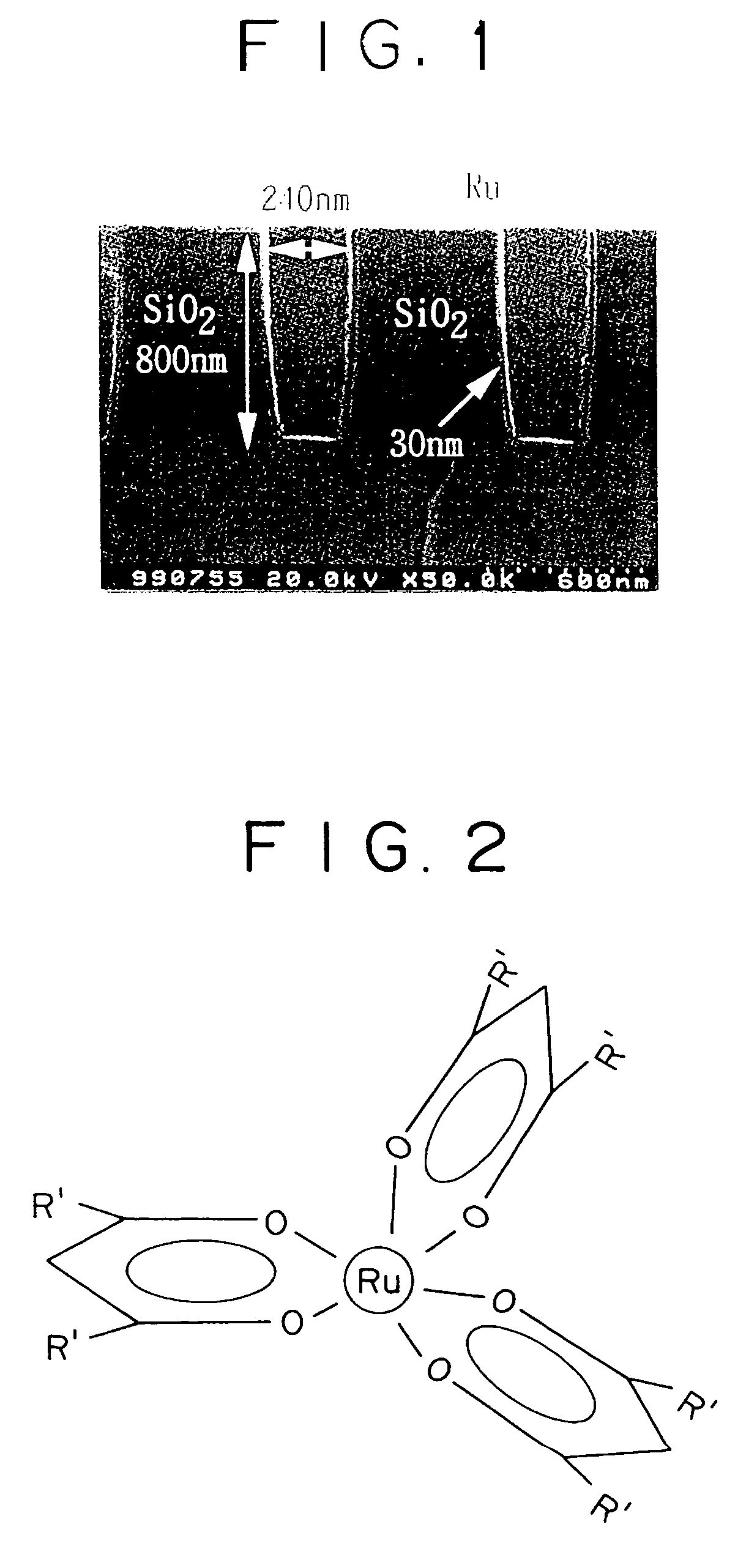
[0038]A method of manufacturing a semiconductor device using a crystal structure shown in FIG. 5 of a discyclopentadienyl ruthenium (RuCP2) complex in which R=H will be described.

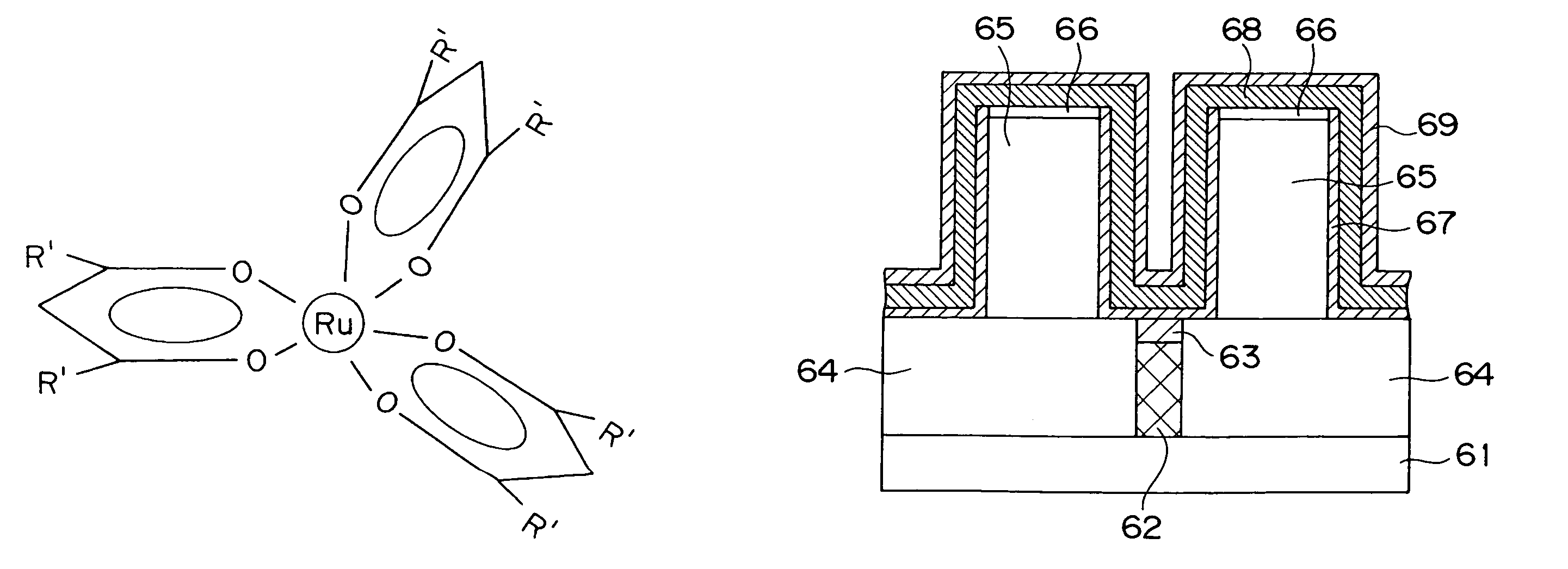
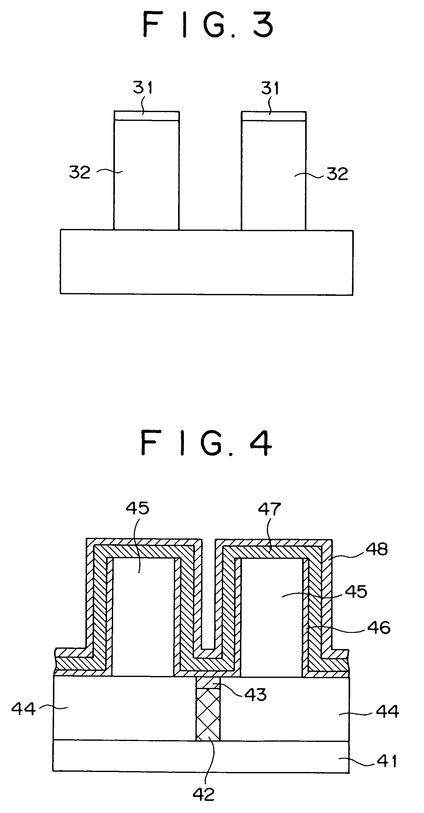
[0039]FIG. 4 is a cross sectional view of a dielectric capacitor contained in a semiconductor device manufactured in accordance with this example. At first, an Si wafer 41 was heated to 300° C. and a contact hole is opened in an SiO2 layer 44 formed by thermal oxidation and then an Si plug 42 is prepared. Then, a barrier layer 43 made of a TiN layer of 100 Å thickness was prepared on the Si plug 42 by a sputtering method. Further, after forming an SiO2 layer 45 of 8000 Å thickness by a plasma CVD process using starting TEOS material, a 2400 Å diameter was fabricated around the contact hole as a center to prepare a substrate having a three-dimensional shape. The aspect ratio (contact hole depth / diameter) of the three-dimensional structure is 3.33.

[0040]A bottom electrode 46 was prepared on the substrate. For...

example 2

[0048]A method of manufacturing a semiconductor device using a crystal structure of the β-diketone complex shown in FIG. 2 of a dibivaloylmethanate ruthenium (Ru(dpm)3) complex in which R′=C(CH3)3 will be described below.

[0049]FIG. 6 is a cross sectional view of a dielectric capacitor contained in a semiconductor device manufactured in accordance with this example. In the same manner as in Example 1, after opening a contact hole to an SiO2 layer 64 formed by thermally oxidizing an Si wafer 61, preparing an Si plug 62 and then forming a TiN barrier layer 63, an insulation layer 65 of an SiO2 layer was prepared to a thickness of 7800 Å by a plasma CVD process. Then, an MgO layer was deposited as an insulation layer 66 by a sputtering process using Mg as a target. A film of 200 Å thickness was obtained by using a 1:1 gas mixture of oxygen and argon as a sputtering gas at a film forming pressure of 2 Pa and with RF power of 200 W. A 2400 Å diameter was fabricated around a contact hole a...

example 3

[0056]A third example of this invention will be explained with reference to FIG. 7.

[0057]FIG. 7 is a cross sectional view of a dielectric capacitor contained in a semiconductor device manufactured in accordance with this example. In the same manner as in Example 1, after opening a contact hole to an SiO2 layer 74 formed by thermally oxidizing an Si wafer 71, preparing an Si plug 72 and then forming a TiN barrier layer 73, an Ru layer was formed by a sputtering process using Ru as a target. A film of 5000 Å thickness was obtained by using an Ar gas as a sputtering gas, at a film forming pressure of 2 Pa and with an RF power of 1200 W. Then, a top electrode 75 having a three-dimensional structure was formed by fabricating a trapezoidal shape around the contact hole as a center. The aspect ratio of the three-dimensional structure is 3.0.

[0058]Then, BST as a dielectric 76 was formed to a 30 nm film thickness on the bottom electrode 75 by an MOCVD process in the same method as in Example...


PUM

PropertyMeasurementUnit
depthaaaaaaaaaa
temperatureaaaaaaaaaa

Abstract

A semiconductor device containing a dielectric capacitor having an excellent step coverage for a device structure of high aspect ratio corresponding to high integration degree, as well as a manufacturing method therefor are provided. A dielectric capacitor of high integration degree is manufactured by forming a bottom electrode 46 and a top-electrode 48 comprising a homogeneous thin Ru film with 100% step coverage while putting a dielectric 47 therebetween on substrates 44, 45 having a three-dimensional structure with an aspect ratio of 3 or more by a MOCVD process using a cyclopentadienyl complex within a temperature range from 180° C. or higher to 250° C. or lower.

Description

CROSS REFERENCE TO RELATED APPLICATION[0001]This application is a continuation application of U.S. Ser. No. 09 / 806,861, filed Apr. 5, 2001 now U.S. Pat. No. 6,821,845, which is a 371 of PCT / JP99 / 05574, filed Oct. 8, 1999, the contents of each of which are incorporated herein by reference.TECHNICAL FIELD[0002]This invention relates to a semiconductor device containing a dielectric capacitor and a method of manufacture thereof; and, more particularly, the invention relates to a semiconductor device in which an electrode comprising Ru, RuO2 or a mixed material of Ru and RuO2 is deposited homogeneously on a substrate with a three-dimensional structure, and a method of manufacture thereof.BACKGROUND OF THE INVENTION[0003]Semiconductor memories include a DRAM (Dynamic Random Access Memory) which is capable of high speed data rewriting. Along with progress in ultra large scale integration technology, the DRAM has entered a large capacity range of 256 M to 1 G bit. Therefore, there has been...

Claims


Application Information

Patent Timeline
Patent Type & Authority Patents(United States)
IPC IPC(8): H01L21/8242C23C16/18C23C16/40H01L21/02
CPCC23C16/18H01L28/60H01L28/55C23C16/40H01L27/04
Inventor NABATAME, TOSHIHIDESUZUKI, TAKAAKIFUJIWARA, TETSUOHIGASHIYAMA, KAZUTOSHI
Owner HITACHI LTD
Why Eureka
Try Eureka