Device used to produce or examine semiconductors

a semiconductor and examining device technology, applied in the direction of individual semiconductor device testing, ohmic-resistance heating, instruments, etc., can solve the problems of inability to easily remove the ceramic substrate, interfere with the temperature control of the ceramic substrate, etc., and achieve the effect of preventing hea

Inactive Publication Date: 2006-07-04
IBIDEN CO LTD
View PDF22 Cites 33 Cited by
  • Summary
  • Abstract
  • Description
  • Claims
  • Application Information

AI Technical Summary

Benefits of technology

[0010]The present invention is completed to solve the above-mentioned problem, and has its object to provide a semiconductor-producing / examining device: which can satisfactorily maintain a connection between a conductor layer formed at a ceramic substrate and an external terminal for a long period of time; and which can easily be removed from a supporting case. It is another object to provide a semiconductor-producing / examining device which can be suitably used as a hot plate, an electrostatic chuck, a wafer prober and the like.
[0013]In the semiconductor-producing / examining device according to the present invention, as described above, the connection between the conductor layer and the external terminal arranged on the surface of the ceramic substrate or inside the ceramic substrate is performed such that the external terminal is pressed on the conductor layer and the like by using elasticity and the like of the elastic body. Therefore, unlike a case in which an external terminal is adhered through a solder material and the like, a defective connection between the external terminal and a conductor layer caused by deterioration of the solder material and the like does not occur. Thus, preferable connection state can be maintained for a long period of time. In addition, since the connection between the conductor layer and the external terminal is performed by bringing the conductor layer and the external terminal into contact with each other, the ceramic substrate can be easily removed from the supporting case.
[0018]In addition, on a face of the ceramic substrate, which is the face opposite to the face for processing the semiconductor, the connection between the conductor layer and the external terminal or the connection between said another conductor layer and the external terminal is desirably performed. This is because heat can be prevented from escaping through the external terminal.

Problems solved by technology

For this reason, the temperature control of the ceramic substrate is interfered.
In this case, a problem that after the ceramic substrate is arranged in a supporting case and a wiring and the like is arranged, the ceramic substrate cannot be easily removed existed.

Method used


Image

  • Device used to produce or examine semiconductors
  • Device used to produce or examine semiconductors
  • Device used to produce or examine semiconductors

Examples


example 1

Producing of Ceramic Heater

[0191](1) A composition comprising 100 parts by weight of aluminum nitride powder (made by TOKUYAMA Corp. , average particle diameter: 1.1 μm), 4 parts by weight of yttrium oxide (Y2O3: yttria, average particle diameter: 0.4 μm), 12 parts by weight of acrylic binder, and alcohol was subjected to spray drying to manufacture granular powder.

[0192](2) The granular powder was put in a mold and formed to have a flat plate form to obtain a raw formed body (green).

[0193](3) The raw formed body subjected to the processing treatment was hot-pressed at a temperature: 1800° C. and a pressure: 20 MPa to obtain an aluminum nitride sintered body having a thickness of 3 mm.

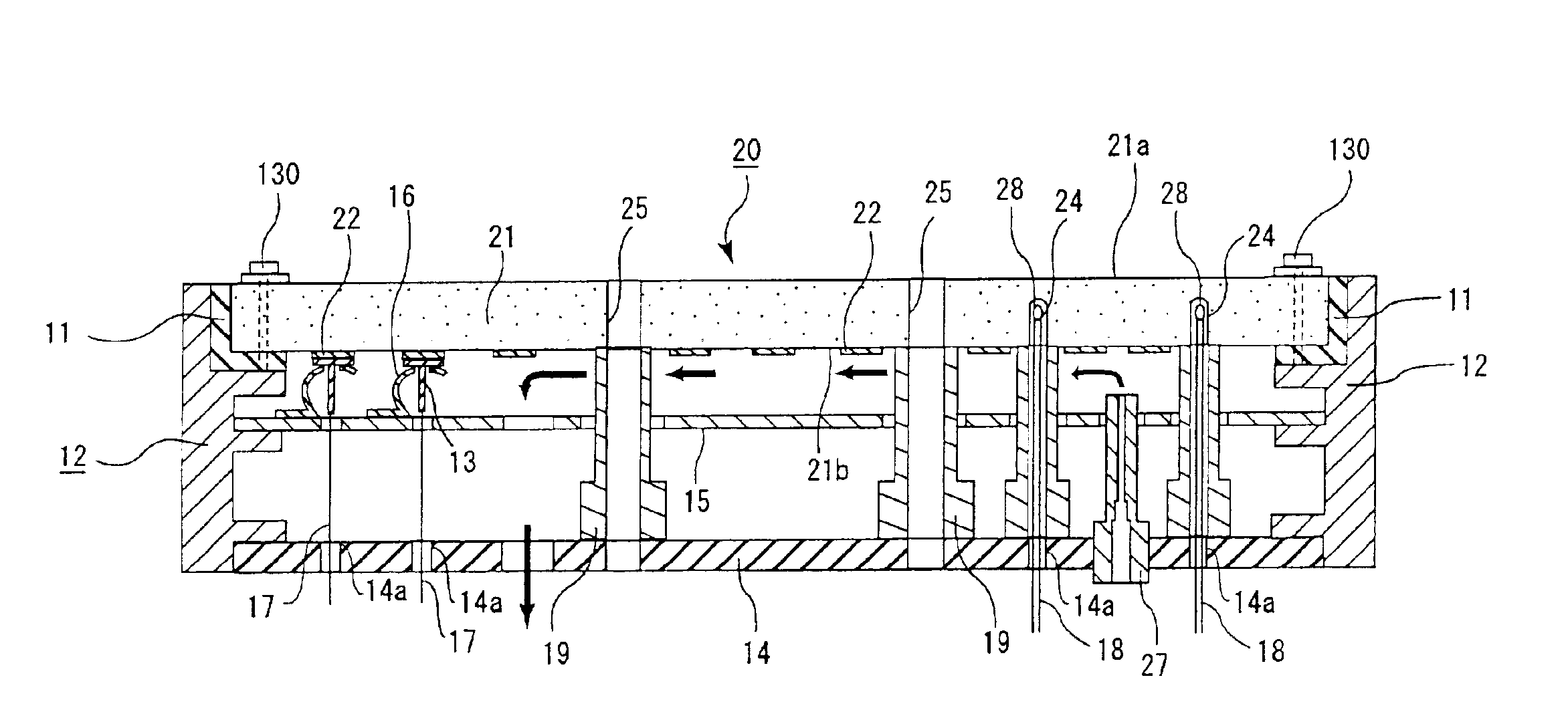
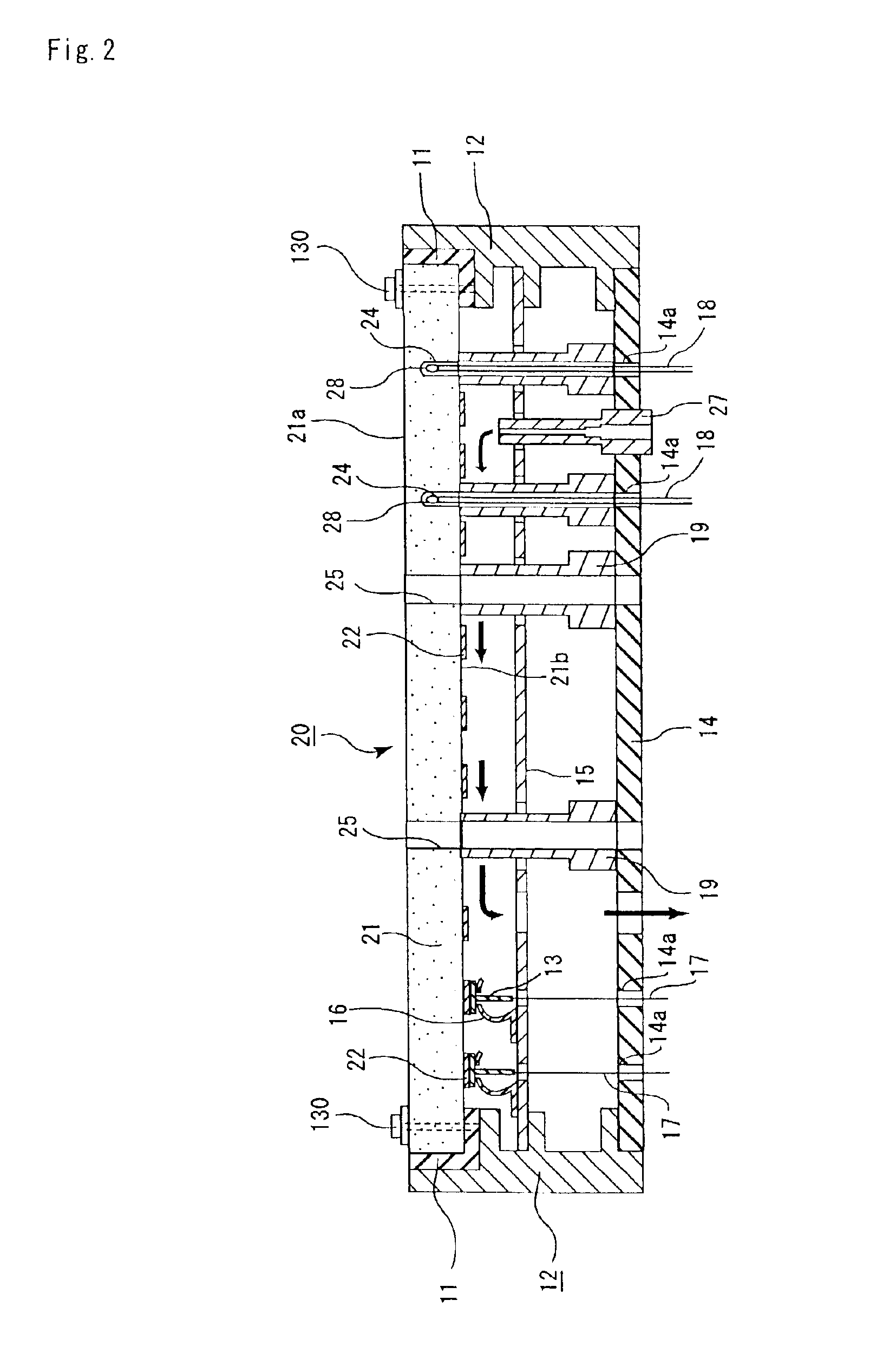
[0194]A disk-like body having a diameter of 210 mm was cut from the sintered body to obtain a plate-formed body (ceramic substrate 21) consisting of a ceramic.

[0195]The plate-formed body was subjected to drilling to form a portion for a through hole in which a lifter pin for a silicon wafer was to be i...

example 2

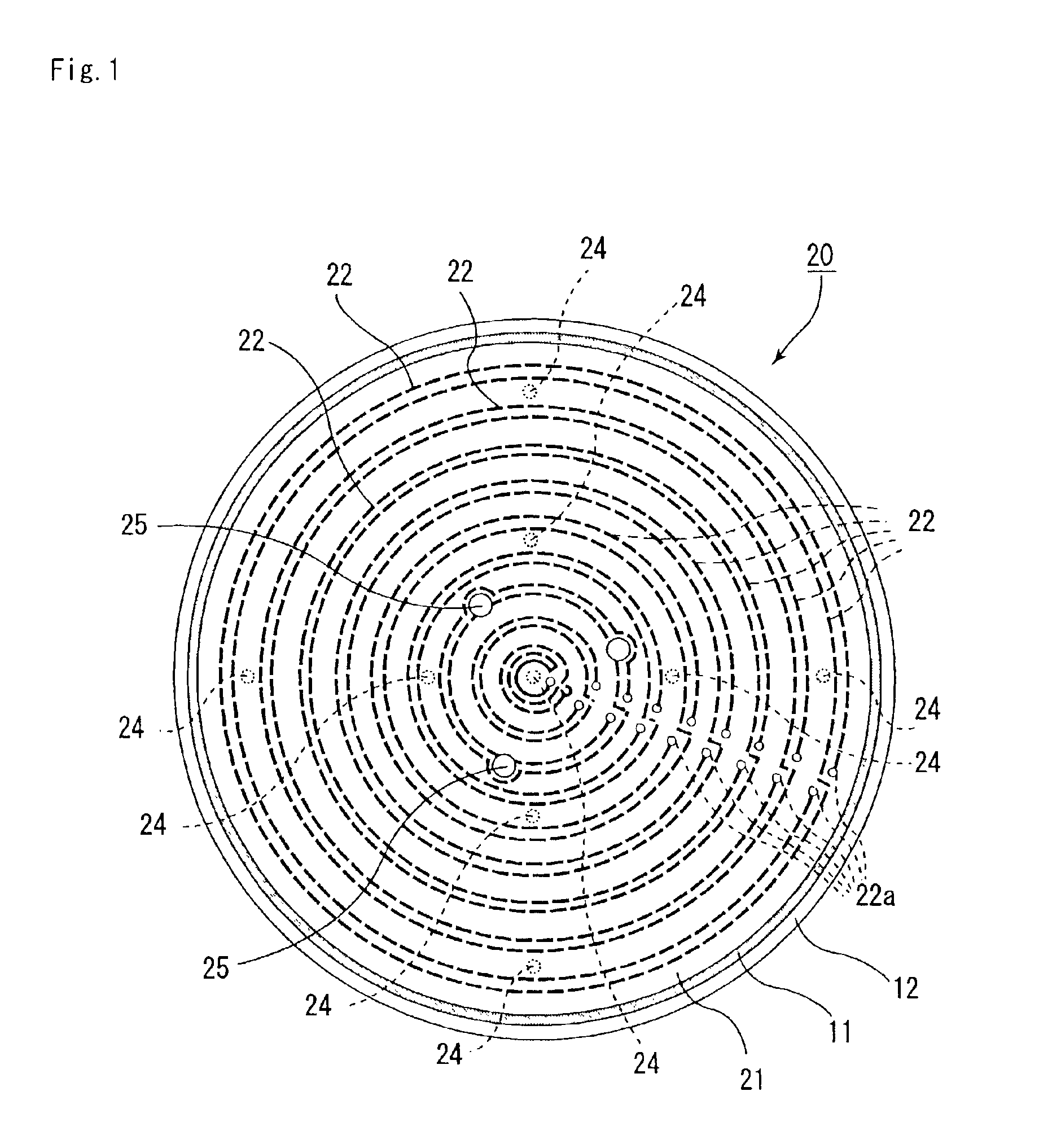
Ceramic Heater (see FIG. 16)

[0204](1) A paste obtained by mixing 100 parts by weight of aluminum nitride powder (made by TOKUYAMA Corp., average particle diameter: 1.1 μm), 4 parts by weight of yttrium oxide (Y2O3: yttria, average particle diameter: 0.4 μm), 11.5 parts by weight of acrylic binder, 0.5 parts by weight of dispersant with 53 parts by weight of alcohol comprising 1-butanol and ethanol was used, and was formed by a doctor blade method to form a green sheet 50 having a thickness of 0.47 mm.

[0205](2) After the green sheet 50 was dried at 80° C. for 5 hours, a portion where a through hole in which a lifter pin for carrying and the like of a silicon wafer was to be inserted, a portion 380 which would be a conductor-filled through hole and the like were formed by punching.

[0206](3) One hundred parts by weight of tungsten carbide particle having an average particle diameter of 1 μm, 3.0 parts by weight of acrylic binder, 3.5 parts by weight of α-Terpineol solvent and 0.3 parts...

example 3

[0216]A ceramic substrate in which a conductor-filled through hole was exposed was produced, and the surface of the exposed conductor-filled through hole was subjected to grinding and the like. Thereafter, the ceramic substrate was subjected to nickel plating and gold plating under the following conditions. Except for these processes, the same processes as those in Example 2 were performed to produce a ceramic heater.

[0217]The ground surface of the conductor-filled through hole was dipped for 20 minutes in an electroless nickel plating solution which had a pH value of 5 and contained 30 g / l of nickel chloride, 10 g / l of sodium hypophosphite, 10 g / l of sodium citrate to form a nickel plating layer 39a having a thickness of 5 μm on the opening part of the conductor-filled through hole. In addition, the resultant structure was dipped in at 93° C. for 23 seconds in an electroless plating bath containing 2 g / l of potassium cyanoaurate, 75 g / l of ammonium chloride, 12 g / l of sodium citrat...


PUM


Abstract

A semiconductor-producing / examining device that can maintain a preferable connection state for a predetermined period of time and that can easily remove a ceramic substrate from a supporting case. The semiconductor producing / examining device includes a ceramic substrate having a conductor layer formed on the surface thereof or inside thereof and a supporting case. An external terminal is connected to the conductor layer. A connection between the conductor layer and the external terminal is performed such that the external terminal is pressed on the conductor layer or the external terminal is pressed on another conductor layer connected to the conductor layer by using the elastic force and the like of an elastic body.

Description

TECHNICAL FIELD[0001]The present invention relates mainly to a semiconductor-producing / examining device used to produce or examine semiconductors such as hot plates (ceramic heaters), electrostatic chucks, wafer probers and the like.BACKGROUND ART[0002]Hitherto, a heater, wafer prober and the like wherein a base material made of metal such as stainless steel or aluminum alloy is used has been used in semiconductor producing / examining devices and so on, examples of which include an etching device, a chemical vapor deposition device and the like.[0003]However, such a heater made of metal has the following problems.[0004]First, the thickness of the heater plate must be made as thick as about 15 mm since the heater is made of metal. Because in a thin metal plate, a bend, a strain and so on are generated on the basis of thermal expansion resulting from heating so that a silicon wafer put on the metal plate is damaged or inclined. However, if the thickness of the heater plate is made thic...

Claims


Application Information

Patent Timeline
Patent Type & Authority Patents(United States)
IPC IPC(8): H01L23/10H01L21/00H01L21/683H01L21/687
CPCH01L21/67103H01L21/68785H01L21/6833
Inventor HIRAMATSU, YASUJIITO, YASUTAKA
Owner IBIDEN CO LTD
Why Eureka
Try Eureka