Method for fabricating a photomask for an integrated circuit and corresponding photomask

a technology of integrated circuits and photomasks, which is applied in the direction of hose connections, couplings, instruments, etc., can solve the problems of high individual layer defect risk of the entire mask system, minimal distance between the produced structures, etc., and achieve the effect of preventing oxidation of the multi-layer coating

Inactive Publication Date: 2006-07-11
POLARIS INNOVATIONS
View PDF4 Cites 78 Cited by
  • Summary
  • Abstract
  • Description
  • Claims
  • Application Information

AI Technical Summary

Benefits of technology

[0024]A particular advantage of the invention is the omission of the absorber layer and of the upper buffer layer. The upper covering layer is optional, but expedient since it can prevent oxidation of the multilayer coating. Since the multilayer deposition is effected after the patterning, the actual structures may already be subjected to a defect inspection, repair and repair qualification beforehand. Consequently, the multilayers are no longer exposed to a further process step after the deposition, or only to the deposition of an upper protection layer.
[0025]In accordance with one preferred embodiment, a plurality of trenches are provided.
[0026]In accordance with a further preferred embodiment, the trench or trenches are provided by means of a photolithographic etching process using a mask, e.g. made of photoresist, and the mask prote...

Problems solved by technology

In microlithography for integrated circuits, there is the problem of configuring the imaging of adjacent openings in the photoresist such that the distance between the structures produced becomes minimal.
A series of technical problems result on account of the abovementioned multilayer arra...

Method used


Image

  • Method for fabricating a photomask for an integrated circuit and corresponding photomask
  • Method for fabricating a photomask for an integrated circuit and corresponding photomask
  • Method for fabricating a photomask for an integrated circuit and corresponding photomask

Examples


first embodiment

[0041]FIGS. 1a–d show successive fabrication steps for a photomask according to the invention as the present invention.

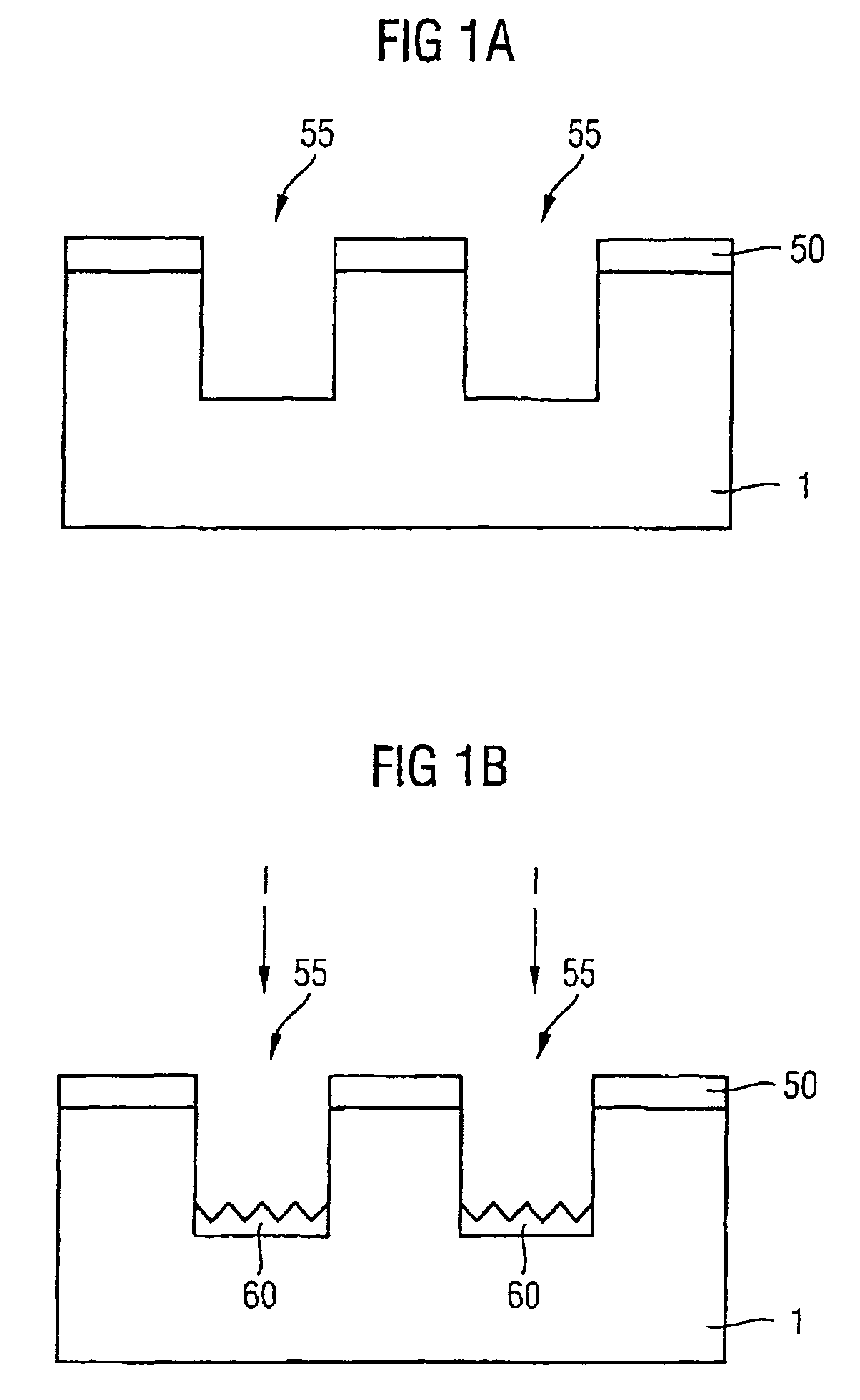
[0042]In accordance with FIG. 1a, a glass substrate 1 is provided, to which a photoresist mask 50 is applied. By means of the photoresist mask 50, trenches 55 are etched into the glass substrate 1, which define the later non-reflective regions.

[0043]In accordance with FIG. 1b, the glass substrate 1 is then subjected to an ion bombardment I using the photoresist mask 50 in order to form porous regions 60 at the bottoms of the trenches 55.

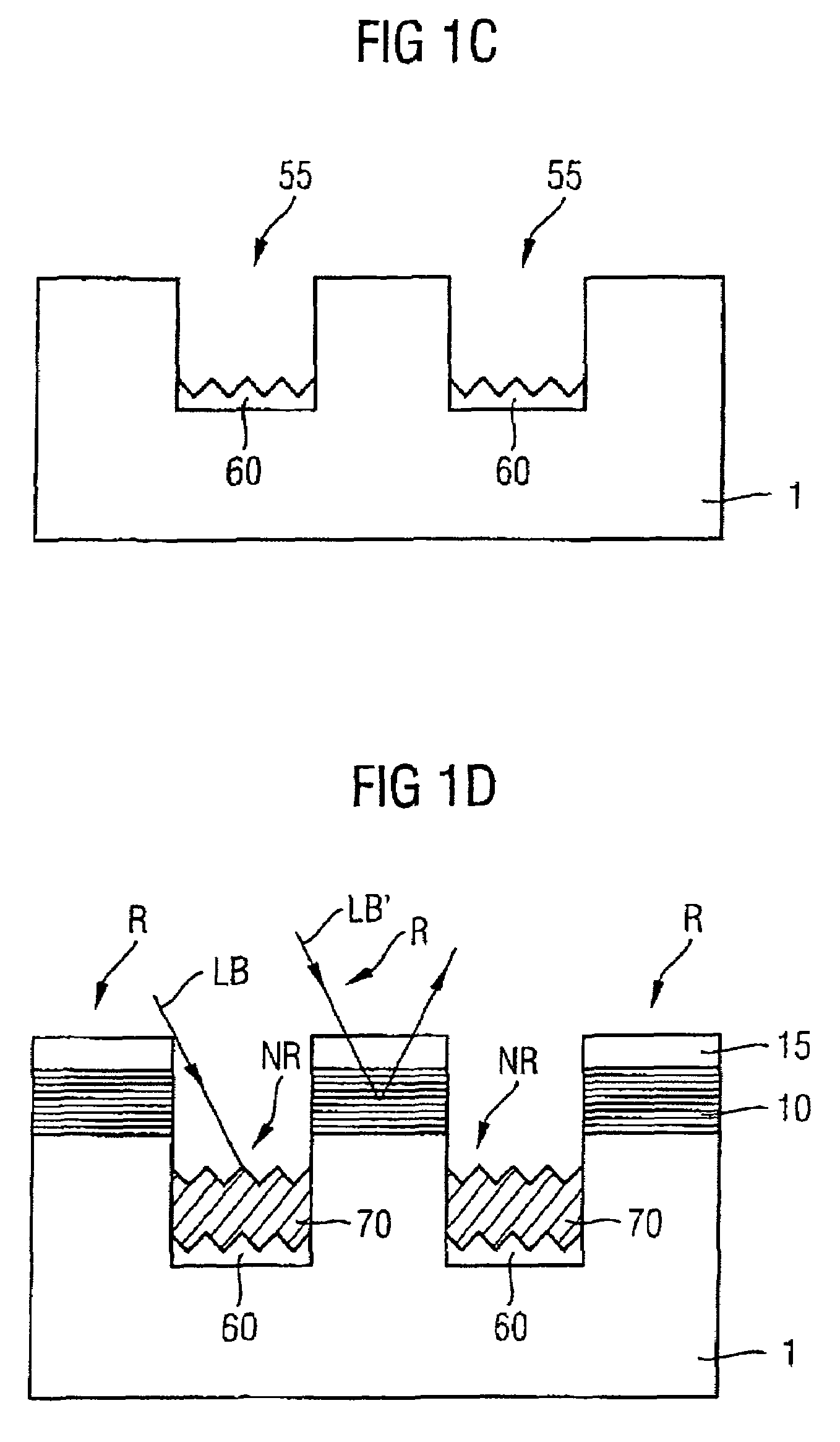
[0044]As shown in FIG. 1c, the photoresist mask 55 is subsequently removed.

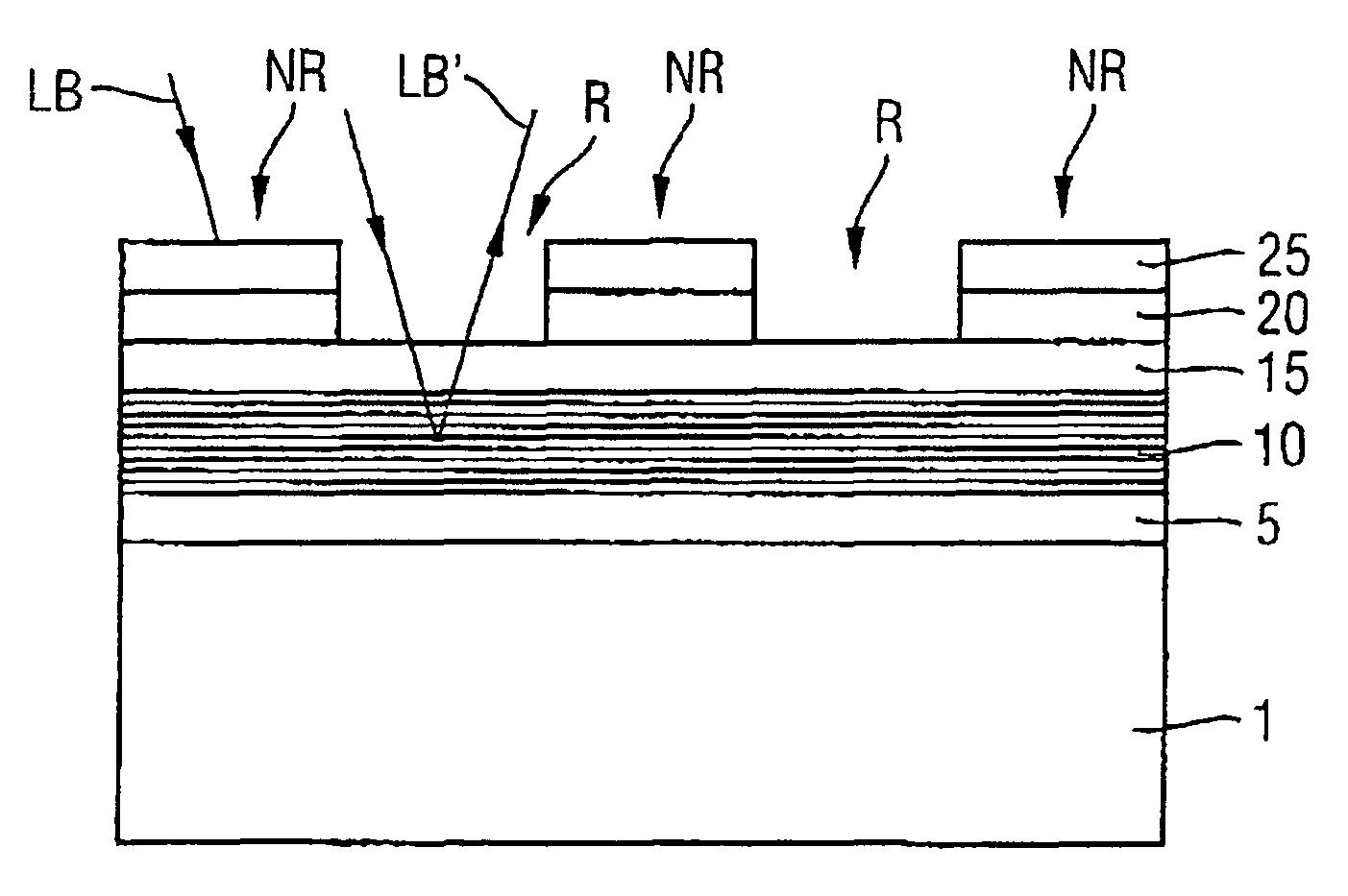
[0045]In the subsequent process step illustrated in FIG. 1d, the multilayer coating 10 is then deposited, to be precise in the present example by alternate sputtering of silicon and molybdenum layers having a thickness of 6.9 nm corresponding to a light wavelength of 13.4 nm.

[0046]Finally, a covering layer 15 e.g. made of silicon having a thickness of 11 nm is...

second embodiment

[0049]FIGS. 2a,b show successive fabrication steps for a photomask according to the invention as the present invention.

[0050]In the second embodiment, use is made of a double substrate 1a, 1b the lower part 1a of which comprises glass and the upper part 1b of which comprises silicon.

[0051]During the trench etching, the upper part 1b made of silicon is not etched through completely, rather a residual thickness d is left in the trenches 55.

[0052]This residual thickness region from the upper part 1b made of silicon is then made porous in an anodic etching process and thus becomes the prepatterned surface region 60′ on which the later multilayer growth is disturbed. A sidewall passivation layer may be deposited beforehand, if appropriate.

[0053]The remaining process steps then proceed in the manner described in the case of the first embodiment above.

[0054]Although the present invention has been described above on the basis of preferred exemplary embodiments, it is not restricted thereto,...


PUM


Abstract

A method for fabricating a photomask for an integrated circuit. The method includes, for example, providing a substrate with at least one trench, providing a prepatterned surface at the bottom of the trench, and providing a multilayer coating over the substrate. As a result, the multilayer coating forms a reflection region on the surface of the substrate outside the trench and a non-reflection region in the trench. The invention additionally provides a corresponding photomask.

Description

CLAIM FOR PRIORITY[0001]This application claims the benefit of priority to German Application No. 102 59 331.0, filed in the German language on Dec. 18, 2002, the contents of which are hereby incorporated by reference.TECHNICAL FIELD OF THE INVENTION[0002]The present invention relates to a method for fabricating a photomask for an integrated circuit and a corresponding photomask.BACKGROUND OF THE INVENTION[0003]In microlithography for integrated circuits, there is the problem of configuring the imaging of adjacent openings in the photoresist such that the distance between the structures produced becomes minimal. Every reduction of the distance leads to a reduction of the chip area, thereby making it possible to reduce the costs per chip.[0004]To date, use has usually been made of binary masks (BIM) or halftone masks HTPSM with lithographically more favorable properties, mainly for projection exposure into a wafer coated with positive resist.[0005]In the foreseeable future, with shor...

Claims


Application Information

Patent Timeline
IPC IPC(8): G01F9/00G03F1/24
CPCB82Y10/00G03F1/24B82Y40/00Y10T403/13
Inventor KAMM, FRANK-MICHAEL
Owner POLARIS INNOVATIONS
Why Eureka
Try Eureka