Method for predicting the behavior of dopant and defect components

a technology of defect components and behavior prediction, applied in stochastic cad, instruments, protective fluids, etc., can solve problems such as kink or non-optimum distribution of boron, degrade performance, and many parts of boron may not have the proper electrical activity, and achieve the effect of higher performance in electronic devices

Inactive Publication Date: 2006-07-11
SEIKO EPSON CORP +1
View PDF1 Cites 5 Cited by
  • Summary
  • Abstract
  • Description
  • Claims
  • Application Information

AI Technical Summary

Benefits of technology

[0013]The distribution of each component that belongs to the first group is predicted by solving the first relationship. Each of the components that belong to the second group is predicted by solving the second relationship. The distribution of each component that belongs to the third group is predicted by solving the first relationship for a time period before the component reaches its pseudo steady state and by solving the second relationship after that time period. The pseudo steady state of a component is a state in which the concentration of that component can be determined by concentrations of other components. The higher the diffusivity or the dissociation rate is, the shorter the duration of the time period is.
[0018]In preferred implementations, the invention thus provides techniques for predicting the structures and properties, such as distribution and clustering of dopants and impurities, that result from implantation, annealing, and other processes for preparing and modifying materials, and for predicting the electrical activity of the system as a function of processing conditions, manufacturing, aging, and application of external fields and conditions. These techniques can be implemented to realize one or more of the following advantages. Accurate prediction of such properties as the distributions of the dopants and defects, electrical activity, critical voltages and fields for electrical or mechanical breakdown, and the effects of aging, and modeling and simulating the structures and properties of devices as a function of processing and operating conditions, can make possible the design of improved composition and processing conditions to develop improved properties, reliability and aging, while minimizing cost and failure. Using these techniques to monitor one or more device characteristics during production and to compare the monitored characteristics to predicted optima can make possible the incorporation of increased automation into control systems for operating the processes. Prediction of performance as a function of aging and operating conditions can make it possible to develop improved fault tolerant systems.

Problems solved by technology

However, it is found that such conditions may lead to a clustering of the dopants and other defects (vacancies and interstitials) and to long-range diffusion tails that degrade the performance, whereas it is desired to maintain the boron near the surface while unclustered in a substitutional site that maximizes performance.
In addition, it is possible that too much of the boron near the surface may diffuse to the interface, resulting in a kink or non-optimum distribution in the boron distribution.
Also, much of the boron may not have the proper electrical activity (as a low energy acceptor level) due to clustering or association with a non-optimum site.
These examples consider boron because there are serious problems today involving such systems; however, similar problems can occur for other dopants.

Method used


Image

  • Method for predicting the behavior of dopant and defect components
  • Method for predicting the behavior of dopant and defect components
  • Method for predicting the behavior of dopant and defect components

Examples


example

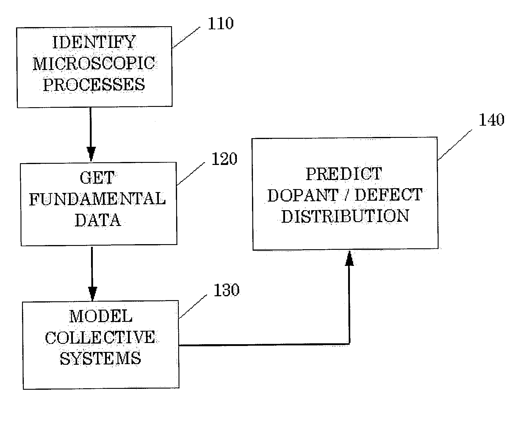
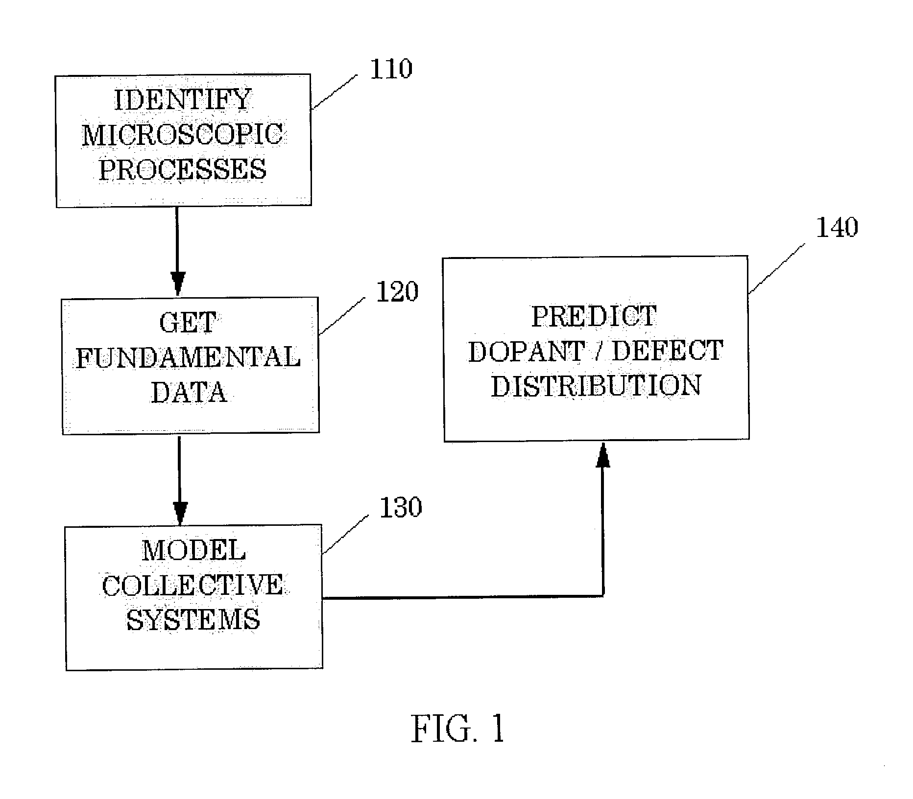
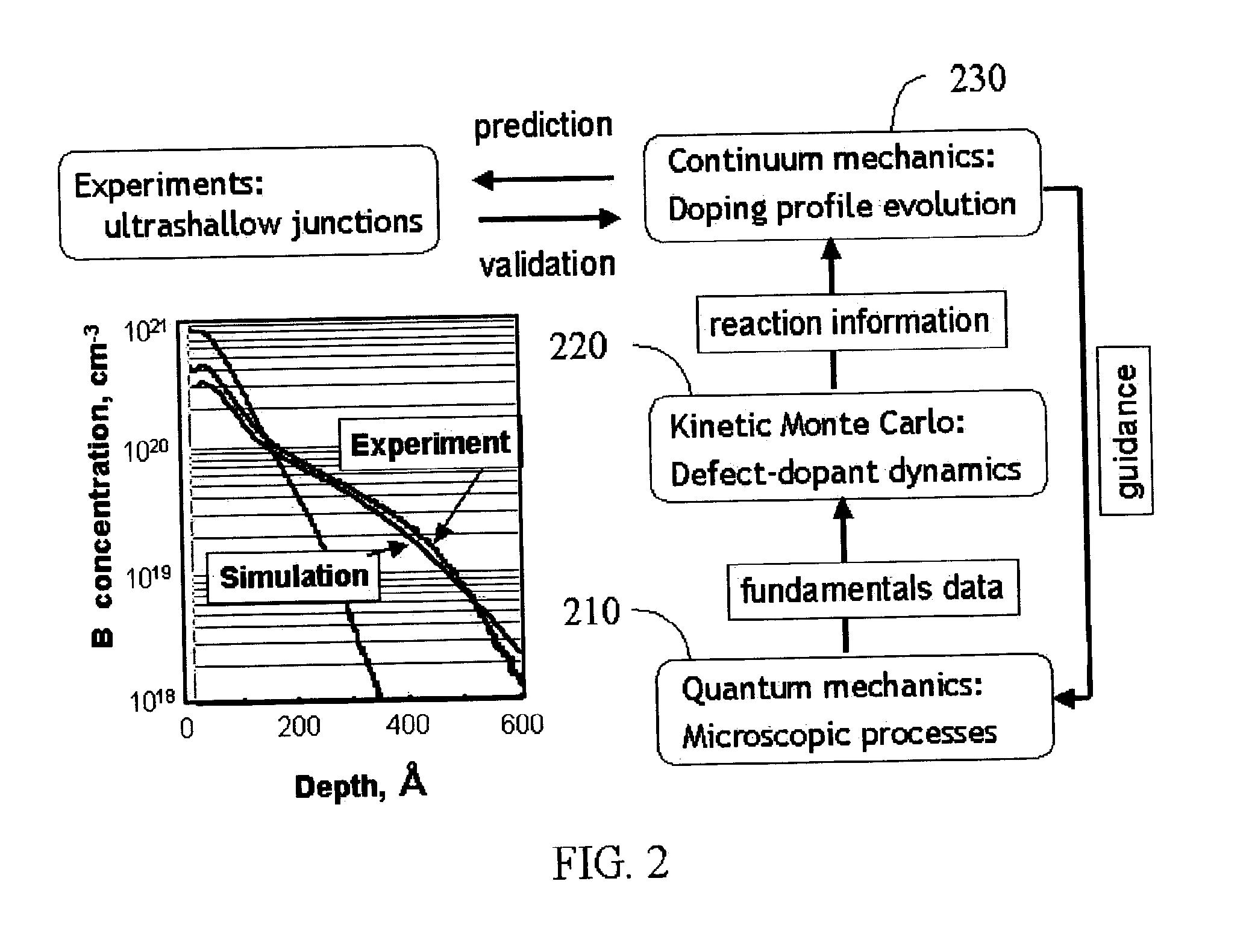
[0038]The following example considers the possible distributions of boron, silicon, and vacancies at various substitutional and interstitial sites, including clusters of several atoms and / or defects at any one site. The application of multiscale modeling for ultra shallow junction processing is summarized in FIG. 2.

[0039]We first used quantum mechanics calculations 210 to model the relevant microscopic processes. All atomic structures were optimized using the local density approximation (LDA) to density functional theory (DFT), as implemented in the CPMD V3.3 package. Calculation of the energetics of the LDA structures using the generalized gradient approximation (GGA) gave similar results. We used a non-local, norm-conserving pseudopotential and a plane-wave cutoff energy of 20 Ry. The defect systems considered were modeled using a 192-atom supercell with a fixed volume that yields a Si—Si bond distance of 2.35 Å in pure silicon. All atomic positions were allowed to relax fully unt...

embodiment 1

[0071]FIG. 4 shows the first example. In this example, boron atoms were implanted on a silicon wafer by implantation energy of 1 keV, and the wafer was annealed for 10 seconds at 1000° C. In this calculation, Eb,BsI was set to be 0.75 eV. The distributions of Bs, BsBi, BsBiI2, Bs2Bi, Bs2Bi2, Bs3Bi, and In were calculated by solving the first relationship, Eq. (1), throughout the simulation, and the distributions of I, BsBiI, BsBi2 and BsBi3 were calculated by solving the second relationship, Eq. (5), throughout the simulation. On the other hand, the distribution of BsI was calculated by solving the first relationship in the time period of t≦0.1 μsec, and by solving the second relationship in the time period of t>0.1 μsec. The distributions of BsI2 and BsI3 were calculated by solving the first relationship in the time period of t≦0.1 msec, and by solving the second relationship in the time period of t>0.1 msec. Finally, the doping profile of boron was obtained by summing up the conce...

embodiment 2

[0072]FIG. 5 shows the second example. In this example, boron atoms were implanted on a silicon wafer by implantation energy of 500 eV, and the wafer was annealed for 10 seconds at 1000° C. In this calculation, Eb,BsI was set to be 0.65 eV. The doping profile of boron was calculated in the same way as that used in Embodiment 1. Experimental data obtained using SIMS measurement is also shown in FIG. 5. Calculated result is in good agreement with experiment.


PUM

PropertyMeasurementUnit
diffusion energy barrieraaaaaaaaaa

Abstract

Techniques for predicting the behavior of dopant and defect components in a substrate lattice formed from a substrate material can be implemented in hardware or software. Fundamental data for a set of microscopic processes that can occur during one or more material processing operations is obtained. Such data can include data representing the kinetics of processes in the set of microscopic processes and the energetics and structure of possible states in the material processing operations. From the fundamental data and a set of external conditions, distributions of dopant and defect components in the substrate lattice are predicted. The distributions of one or more fast components are each predicted by calculating the concentration of the particular fast component for a time period before that fast component reaches its pseudo steady state by solving a first relationship and calculating the concentration of that fast component after the time period by solving a second relationship based on other components, the pseudo steady state of a fast component being a state in which the concentration of that fast component is determined by concentrations of other components. The distribution of Bs3Bi, in addition to the distributions of Bs, BsI, BsI2, BsI3, BsBi, BsBi2, BsBi3, BsBiI, BsBiI2, Bs2Bi, Bs2Bi2, I and In, are calculated by solving the first relationship to predict the distribution of boron after annealing, where Bs and Bi represent substitutional boron and interstitial boron, respectively, and I and In represent interstitial silicon and a cluster of n I's, respectively.

Description

RELATED APPLICATION DATA[0001]This application is related to application Ser. No. 10 / 113,919 (Pub. No. 2002 / 0188373 A1) filed on Mar. 28, 2002 in the names of William A. Goddard III and Gyeong S. Hwang. The contents of this related application is incorporated by reference herein.BACKGROUND OF THE INVENTION[0002]1. Field of the Invention[0003]The invention relates to semiconductor processing and the prediction of structures and properties resulting from processes used in the preparation and modification of semiconductor materials. The prediction can be embodied in methods which can be implemented in hardware or software.[0004]2. Description of the Related Art[0005]In order to maximize the performance and value of electronic devices including memories, central processor units (CPUs), transmitters and detectors of electromagnetic and sonic radiation, and other components of electronic computers, it is important to reduce the size, noise, and reproducibility while increasing the speed o...

Claims


Application Information

Patent Timeline
Patent Type & Authority Patents(United States)
IPC IPC(8): C30B1/00H01L21/22G06F17/50H01L21/265
CPCG06F17/5018H01L21/26513G06F2217/10G06F30/23G06F2111/08H01L21/26566H01L21/2658
Inventor SATO, YUZURUUEHARA, MASAMITSUHWANG, GYEONG S.GODDARD, III, WILLIAM A.
Owner SEIKO EPSON CORP
Why Eureka
Try Eureka