Semiconductor apparatus and process of production thereof

a technology of semiconductor devices and semiconductor chips, applied in the direction of electrical devices, semiconductor/solid-state device details, semiconductor devices, etc., can solve the problems of thermal stress becoming a major disadvantage for the reliability of the joint, the formation of uniform solder bumps of the same height in the semiconductor chip is extremely difficult, and the solder bump formation is difficult. to achieve the effect of reliable joining by soldering, reduced connection resistance and increased joint strength

Inactive Publication Date: 2006-07-18
SONY CORP
View PDF9 Cites 9 Cited by
  • Summary
  • Abstract
  • Description
  • Claims
  • Application Information

AI Technical Summary

Benefits of technology

[0083]Further, by forming the solder layers by a eutectic solder, the wettability with the eutectic solder precoated on the connection lands of the mounting board becomes excellent and reliable joining by soldering is achieved.
[0084]Further, since the surfaces of the solder bumps are cleaned by the plasma cleaning, the connection resistance is reduced and the joint strength is increased at the joint portions of the solder bumps and the solder layers.
[0085]Therefore, in the mounting of a semiconductor device to the mounting board, the thermal stress is relieved and the connection resistance is reduced and joint strength increased, whereby mounting defects are greatly reduced and the reliability of the joint portions by the metal bumps is improved.
[0086]Further, since the formation of the metal bumps and formation of the resin film and the plasma cleaning or laser beam irradiation and, in some cases, the formation of the solder layers are performed on a semiconductor device when at least three steps are performed on a semiconductor device formed on a semiconductor substrate in the semiconductor wafer state, there is no need to perform this work on the individual semiconductor devices, it is possible to perform this work on a large number of semiconductor devices at one time, and the productivity is improved more.

Problems solved by technology

In this case, there is the disadvantage that the thickness of the solder bumps formed is affected by the surface conditions of the layer of material forming the underlayer of the bumps or the slight variation in the electrical resistance and that the formation of uniform solder bumps of the same height in a semiconductor chip is extremely difficult.
The thermal stress becomes a major disadvantage for the reliability of the joint by the bumps after flip-chip mounting due to the differences in the coefficients of heat expansion of the semiconductor chips and the mounting board (printed circuit board).
While the coefficient of heat expansion of silicon is 3.4 ppm / ° C., the coefficient of heat expansion of the generally widely used glass epoxy-based mounting board is a large about 15 ppm / ° C. When thermal stress is repeatedly applied to bump joints by the temperature difference caused by the on / off operation of a chip, cracks are caused in the joints and breakage or malfunctions are caused in some cases.
In the above flip-chip mounting method of the related art, however, since the semiconductor chips and the mounting board are secured by a sealing resin, when a defect occurs in a device chip, the only method was to discard the entire mounting board 2 on which that semiconductor chip 1 was mounted or apply a chemical or mechanical external force to forcibly tear off that semiconductor chip.
Here, the replacement of the entire mounting board 2 of the former case has the disadvantage of the cost ending up higher, while the forcibly tearing off of the semiconductor chip 1 of the latter case ends up damaging the mounting board 2.
Therefore, the work of replacing a defective component in the case of a defect occurring in a semiconductor chip 1, that is, the so-called rework, is difficult.
This has become one factor behind the failure of flip-chip mounting from spreading widely.
Further, along with the reduction of pitch accompanying the reduction of size of semiconductor devices, at the time of injection of the sealing resin, the circulation of the sealing resin 3 becomes poor and full injection of the sealing resin 3 can no longer be achieved, so there is also the disadvantage that the thermal stress cannot be sufficiently relieved.

Method used


Image

  • Semiconductor apparatus and process of production thereof
  • Semiconductor apparatus and process of production thereof
  • Semiconductor apparatus and process of production thereof

Examples


first embodiment

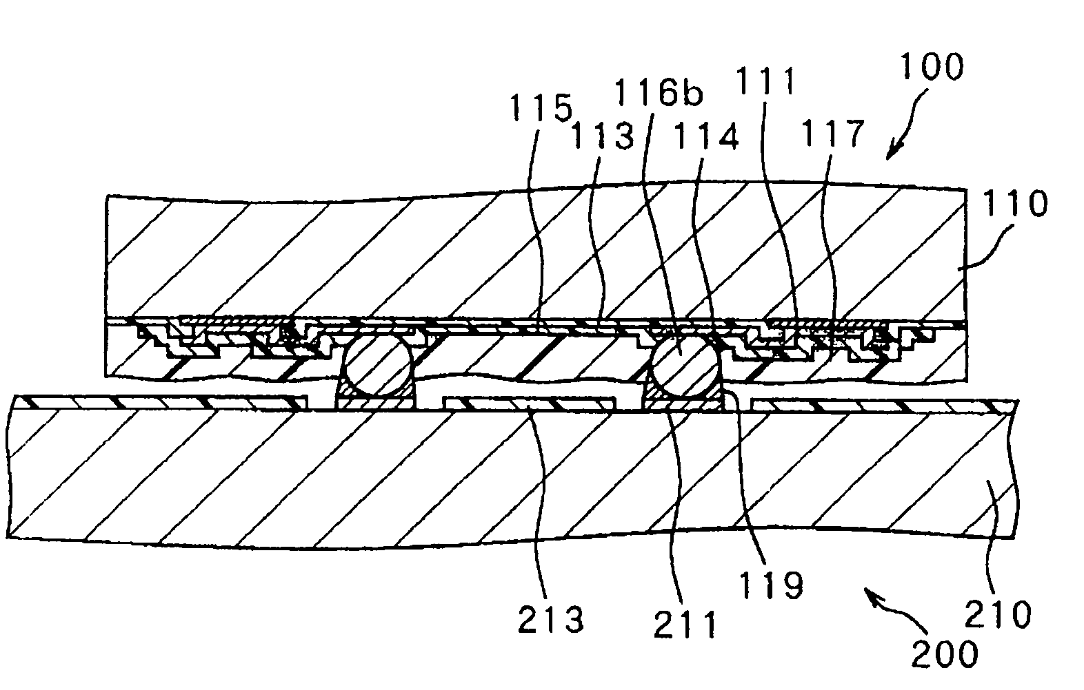
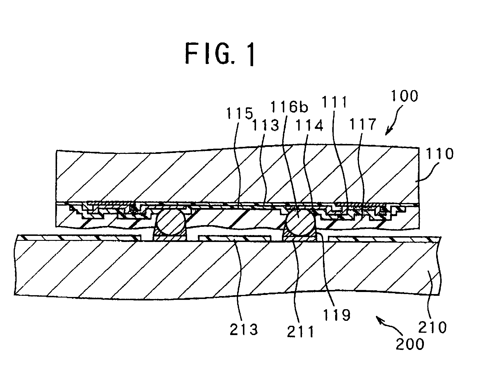
[0107]FIG. 1 is a sectional view of a semiconductor apparatus produced by the process of production of a semiconductor apparatus according to the present embodiment.

[0108]The surface of the semiconductor chip 110 for forming the electrode pads 111 comprised of aluminum etc. is for example covered by a surface protective film 113 comprised of for example a silicon nitride layer or polyimide layer, then electrode pad 111 portions are opened.

[0109]A conductive film 114 comprised of a stacked film of chrome, copper, and gold etc. is formed at the openings connected to the electrode pads 111. The conductive film is sometimes called a BLM (Ball Limiting Metal) film. Further, an upper surface protective film 115 comprised of for example a polyimide is formed on the conductive film (BLM film) 114 and bump forming areas are opened.

[0110]In the above bump forming regions, bumps 116b comprised of for example high melting point solder balls are formed connected to the conductive film (BLM film)...

second embodiment

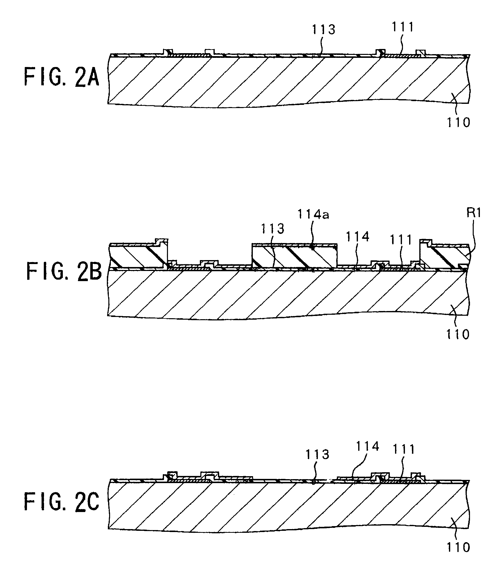
[0198]FIG. 8 is a view for explaining a second embodiment of the process of production of a semiconductor apparatus according to the present invention.

[0199]The point of difference of the second embodiment from the first embodiment explained above is that the cleaning of the surfaces of the bumps 116b exposed from the resin film 117 is performed by removing the resin film and other unnecessary components by irradiation of a laser beam L as shown in FIG. 8 instead of plasma cleaning.

[0200]The processing of the rest of the steps is performed in the same way as the first embodiment. That is, in the second embodiment, the step shown in FIG. 8 is performed instead of the step of FIG. 4C in the process of production explained with relation to FIGS. 2A, 2B, and 2C, FIGS. 3A, 3B, and 3C, FIGS. 4A, 4B, and 4C, and FIGS. 5A and 5B.

[0201]Further, since a semiconductor apparatus similar to the semiconductor apparatus shown in FIG. 1 is obtained by this process of production, a detailed explanat...


PUM


Abstract

A process of production of a semiconductor apparatus which can suppress a rise in the electrical resistance and a decline in the joint strength at the bump connection interfaces and improve the connection reliability when using the method of reinforcing the bases of the bumps by a resin film. Bumps are formed on a semiconductor wafer formed with a pattern circuit of a semiconductor chip so as to connect to the circuit pattern, a resin film is formed on the bump forming surface of the semiconductor wafer to a thickness giving a surface lower than the height of the bumps while sealing the spaces between the bumps, plasma cleaning etc., is used to remove the sealing resin components deposited on the surface portions of the bumps or natural oxides or other insulating impurities to clean and activate the surfaces of the bumps, and the chip is mounted on a mounting board.

Description

RELATED APPLICATION DATA[0001]This application is a divisional application Ser. No. 09 / 385,959 filed Aug. 30, 1999. The present and foregoing application claims priority to Japanese Application No. P10-247393 filed Sep. 1, 1998 and Application No: P11-146942 filed May 26, 1999. All of the foregoing applications are incorporated herein by reference to the extent permitted by law.BACKGROUND OF THE INVENTION[0002]1. Field of the Invention[0003]The present invention relates to a semiconductor apparatus mounted using solder or other metal bumps and a process of production of the same.[0004]2. Description of the Related Art[0005]In recent years, digital video cameras, digital cellular phones, notebook-type personal computers, and other portable electronic equipment have spread widely. There are mounting demands for reducing the size, reducing the thickness, and reducing the weight of these portable electronic equipment.[0006]To realize this reduction in size, reduction in thickness, and r...

Claims


Application Information

Patent Timeline
Patent Type & Authority Patents(United States)
IPC IPC(8): H01L29/40H01L21/60H01L21/56H01L23/04H01L23/31
CPCH01L21/56H01L23/3114H01L24/03H01L24/11H01L24/12H01L24/16H01L2924/13091H01L2924/10253H01L2224/136H01L2924/01072H01L2924/01033H01L2924/01024H01L2924/01005H01L2924/00013H01L2924/19041H01L2924/14H01L2924/014H01L2924/01322H01L24/02H01L2224/0231H01L2224/0401H01L2224/1147H01L2224/13022H01L2224/13116H01L2224/16225H01L2224/73204H01L2924/01002H01L2924/01004H01L2924/01006H01L2924/01013H01L2924/01014H01L2924/01015H01L2924/01018H01L2924/01029H01L2924/01047H01L2924/0105H01L2924/01078H01L2924/01079H01L2924/01082H01L2224/13099H01L2924/00H01L2924/351H01L2924/181H01L2924/12042H01L2224/73104H01L2924/0001H01L24/05H01L24/13H01L2224/05548H01L2224/13024H01L2224/02377H01L2224/02311H01L2224/02H01L23/04
Inventor YANAGIDA, TOSHIHARU
Owner SONY CORP
Why Eureka
Try Eureka