Method for attaching rod-shaped nano structure to probe holder

Inactive Publication Date: 2006-08-01
KOREA INST OF MASCH & MATERIALS
View PDF6 Cites 37 Cited by
  • Summary
  • Abstract
  • Description
  • Claims
  • Application Information

AI Technical Summary

Benefits of technology

[0022]It is, therefore, an object of the present invention to solve the foregoing problems by providing a probe, which is capable of detecting a surface signal or a chemical signal through a rod-shaped nano structure such as tungsten nanowire, carbon nanotube, boron nanotube and the like attached to a tip end portion of the probe, a

Problems solved by technology

However, it is very difficult to individually form a high quality carbon nanotube in a desired shape at a desired position.
It is very difficult to purify, separate and manipulate such an entangled nanotube so as to be attached to a single device.
Even though such methods are effective for developing a new complex material by massively producing the carbon nanotube or carbon fibril, it is almost impossible to separate individual nanotube and precisely attach each one to a desired position, as stated above.
Thus, it is inappropriate to mount a nanotube tip on the probe of the AFM as a commercial method.
However, it is very difficult to attach catalyst particles to the tip of the silicon pyramid.
Although discharging methods are used to reduce the size, they rarely succeed in precisely adjusting the size.
However, all of these methods pose a problem in that coating the precursor exactly to a desired amount is very difficult primarily because of mechanical and chemical properties of the precursor.
Unfortunatel

Method used


Image

  • Method for attaching rod-shaped nano structure to probe holder
  • Method for attaching rod-shaped nano structure to probe holder
  • Method for attaching rod-shaped nano structure to probe holder

Examples


first embodiment

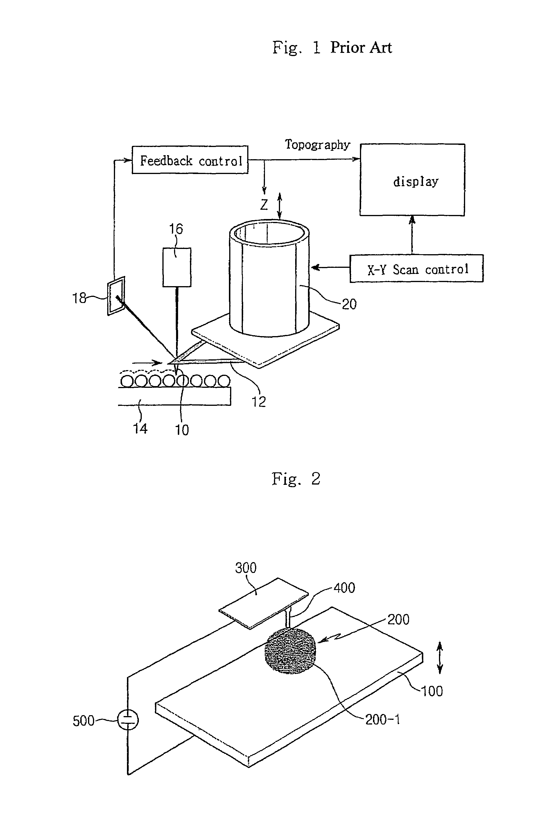
[0035]FIG. 2 is a view for explaining the method for producing a probe with a rod-shaped nano structure attached according to the present invention.

[0036]Referring to FIG. 2, well-conductive electrodes 100 are disposed. Preferably, material with a high conductivity, e.g. Au, Ag, Al, Cu, Ti, and the like, is utilized for the electrodes. On the top portion of the electrodes is a supporter 300, which is also conductive and made of a conductor or coated with a conductor, maintaining a predetermined distance from the electrodes in a horizontal direction. The supporter is usually made of silicon, and to apply the electrodes to this silicon supporter, the supporter can be coated with the metals mentioned above. A holder 400, operating as an electrode, is disposed at a lower portion of the supporter 300, again maintaining a predetermined distance from the electrodes 100. The holder and the supporter can be combined to each other. In such case, silicon is often used to form the shape, and si...

second embodiment

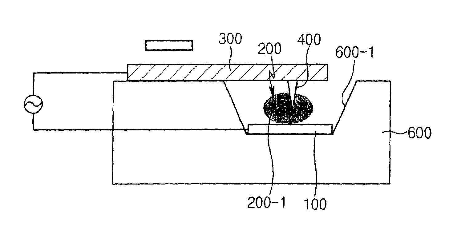
[0049]FIGS. 5a to 5c are views for explaining the method for producing a probe with the rod-shaped nano structure attached according to the present invention.

[0050]With reference to the drawings, a substrate 600 having a groove 600-1 is disposed on a central part of a probe, and electrodes 100 are placed on a top surface of the trench 600-1. The electrodes 100 are formed by coating with layers according to a deposition process, and the substrate 600 for forming the trench 600-1 is layered thereon. Here, the trench can be formed using a general etching process. Since the electrodes and the substrate are made of different materials, the electrodes are etched until they are exposed. On the top portion of the electrodes 100 is a supporter 300, which is conductive and made of conductive materials or coated with a conductor, maintaining a predetermined distance from the electrodes in a horizontal direction. A holder 400, acting as an electrode, is disposed at the lower surface of the supp...

third embodiment

[0056]FIGS. 6a to 6d are views for explaining the method for producing a probe with a rod-shaped nano structure attached according to the present invention.

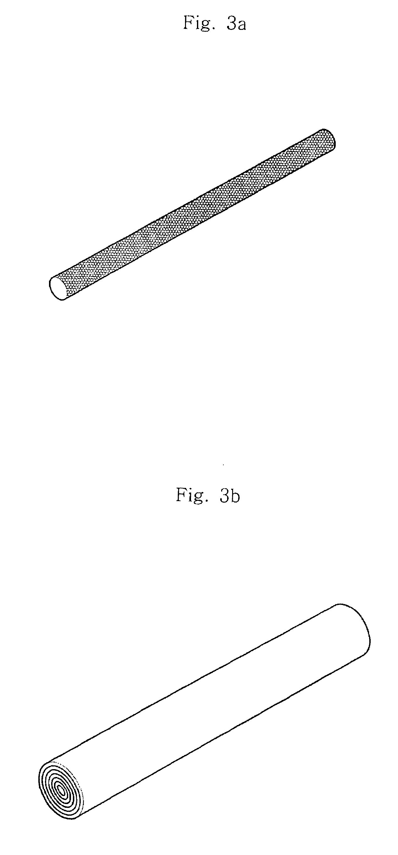
[0057]As depicted in FIG. 6a, a substrate 600 is installed, and a holder 800 composed of two metal electrodes coated with metals are disposed on both sides of a top surface of the substrate, keeping a predetermined distance from the center. As shown in FIG. 6d, a lower end portion (or base end portion) of the holder 800 to be etched is coated with a sacrificial layer in advance, to etch and lift the holder 800 through a Lift-off process.

[0058]Now turning to FIG. 6b, the solution in which the rod-shaped nano structure 200-1 is dispersed is dropped into between the two electrodes on the substrate 600. At this time, the solution 200 is dropped until adjacent end portions of those two electrodes are immersed into the solution. Then applying a voltage to those two metal electrodes, an electric field is generated between the two electr...


PUM

PropertyMeasurementUnit
Lengthaaaaaaaaaa
Structureaaaaaaaaaa

Abstract

The present invention relates to a method for manufacturing a probe for detecting surface signals or chemical signals through a long and slender rod-shaped nano structure such as tungsten nanowire, carbon nanotube, boron nanotube, etc., being attached to a tip end portion thereof. According to the method, a holder, acting as the probe, including a first electrode to which the rod-shaped nano structure is attached, and a second electrode at a predetermined distance from the first electrode are partially or fully immersed in a solution containing the rod-shaped structure. When a voltage is applied between two electrodes, an electrical field is generated, and the rod-shaped nano structure is attached to the holder, acting as the probe.

Description

BACKGROUND OF THE INVENTION[0001]1. Field of the Invention[0002]The present invention relates to a probe for signal detection having a rod-shaped nano structure attached thereto and a method for manufacturing the same, and more particularly, to a probe for detection of a surface signal or a chemical signal having a rod-shaped nano structure, such as tungsten nanowire, carbon nanotube, boron nanotube, etc., which is attached to an tip portion thereof and a method for manufacturing the same.[0003]2. Description of the Related Art[0004]Until recently, the nano world of atom or molecular unit was an unknown field as being too minute to be observed even by a microscope of a high resolution. With introduction of an SPM (scanning probe microscope) in 1980s, however, the nano world finally has become structurally identified. The first kind of atomic microscope such as the SPM was an STM (scanning tunneling microscope) while the most commonly used one is an AFM (atomic force microscope).[000...

Claims


Application Information

Patent Timeline
IPC IPC(8): H01R43/16G01Q60/16B82B3/00G01D21/00G01Q60/22G01Q60/38G01Q70/12G01Q70/16
CPCB82Y15/00B82Y30/00B82Y35/00G01Q70/12Y10T29/49002Y10T29/49117Y10T29/49204
Inventor HAN, CHANG SOOLEE, EUNG SUGLEE, HYUNG-WOO
Owner KOREA INST OF MASCH & MATERIALS
Why Eureka
Try Eureka