

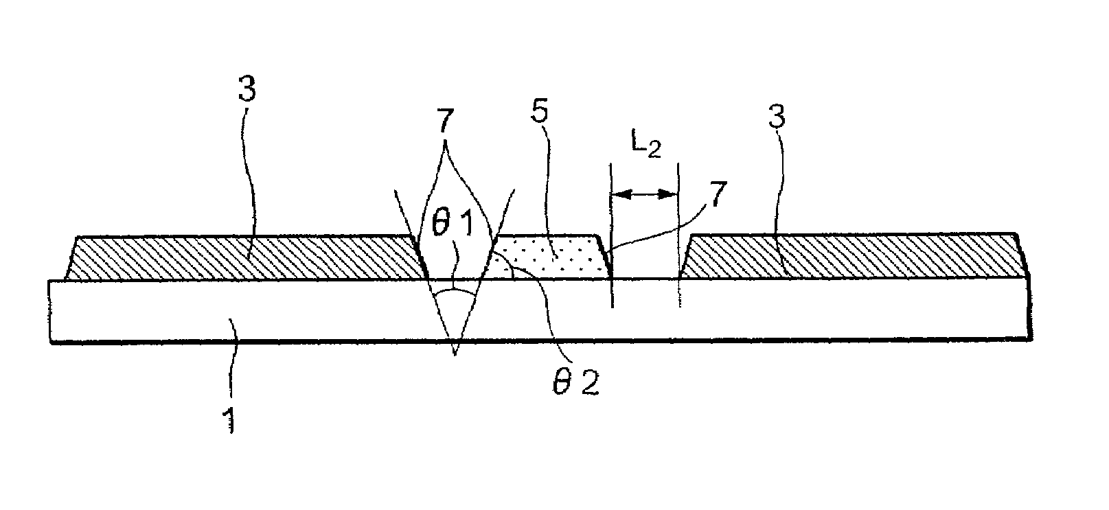
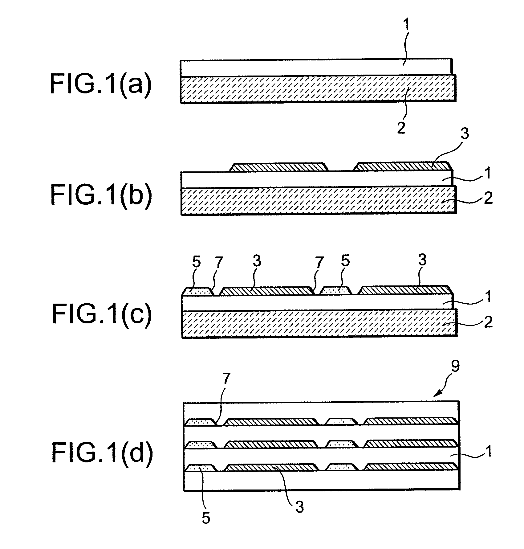
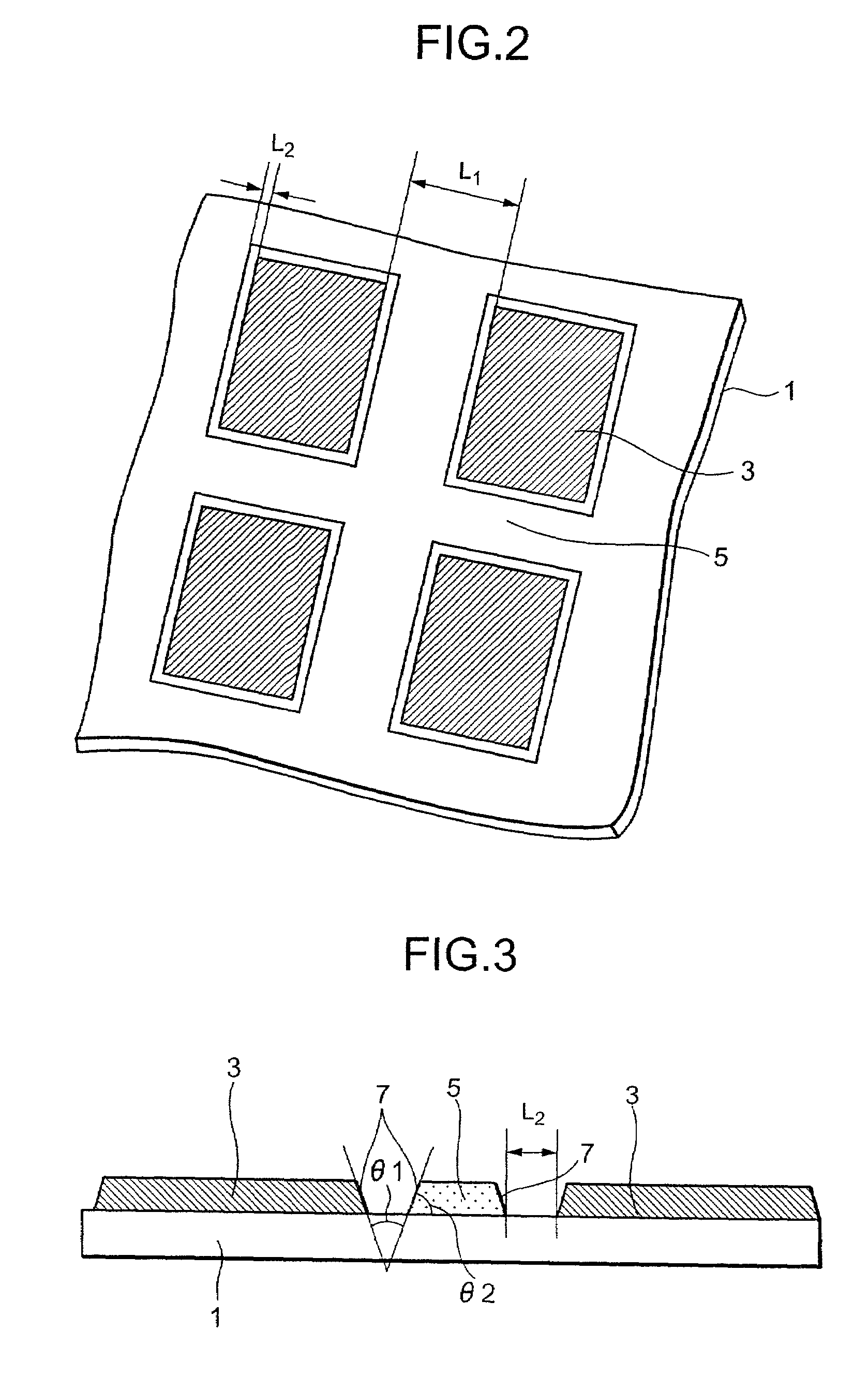
Method of producing ceramic laminates
a technology of ceramic laminates and laminates, applied in the direction of film/foil adhesives, printed circuit assembling, fixed capacitors, etc., can solve the problems of reducing the adhesion of ceramic green sheets in the portions, and affecting the production efficiency of ceramic green sheets. , to achieve the effect of suppressing the occurrence of delamination and cracks, suppressing the occurrence of ceramic laminates, and increasing the number of laminated
- Summary
- Abstract
- Description
- Claims
- Application Information
AI Technical Summary
Benefits of technology
Problems solved by technology
Method used
Image

Examples
example 1
[0245]A laminated ceramic capacitor which is a ceramic laminate was produced in a manner as described below.
[0246]To 100 mol parts of a composition comprising 99.5 mol % of BaTiO3 and 0.5 mol % of MnO, there were added 0.5 mol parts of Y2O3 and 0.5 mol parts of MgO. To 100 parts by weight of this ceramic component was added 55% by weight of a vehicle comprising 5.5% by weight of an ethyl cellulose and 94.5% by weight of a petroleum alcohol. The mixture was kneaded by using a three-roll mill to prepare a ceramic slurry which was, then, applied onto a belt-like carrier film of a polyester by a die coater method to prepare a ceramic green sheet.
[0247]An electrically conducting paste was prepared by kneading 45% by weight of a nickel powder having a particle diameter of 0.2 μm, and 55% by weight of a vehicle comprising 5.5% by weight of an ethyl cellulose and 94.5% by weight of a petroleum alcohol by using a three-roll mill.
[0248]A ceramic paste for forming ceramic patterns was prepared...
example 2
[0268]A laminated ceramic capacitor was produced in a manner as described below.
[0269]To 100 mol parts of a composition comprising 99.5 mol % of BaTiO3 and 0.5 mol % of MnO, there were added 0.5 mol parts of Y2O3 and 0.5 mol parts of MgO. To 100 parts by weight of this ceramic component was added 55 parts by weight of a vehicle comprising 5.5% by weight of a polyvinyl butyral, 1.7% by weight of a plasticizer and 92.8% by weight of a petroleum alcohol. The mixture was kneaded by using a ball mill to prepare a ceramic slurry which was, then, applied onto a belt-like carrier film of a polyester by a die coater method to prepare a ceramic green sheet. The thickness of the ceramic green sheet was adjusted to be about 2.5 μm.
[0270]An electrically conducting paste was prepared by kneading 45% by weight of a nickel powder having an average particle diameter of 0.2 μm, and 55% by weight of a vehicle comprising 5.5% by weight of an ethyl cellulose and 94.5% by weight of a petroleum alcohol by...
example 3
[0294]A laminated ceramic capacitor was produced in a manner as described below.
[0295]To 100 mol parts of a composition comprising 99.5 mol % of BaTiO3 and 0.5 mol % of MnO, there were added 0.5 mol % of Y2O3 and 0.5 mol % of MgO, and to which was further added a glass powder having a softening point and in an amount as shown in Table 3 to prepare a dielectric ceramic slurry. The dielectric ceramic slurry was applied onto a belt-like carrier film of a polyester by a die coater method to prepare a dielectric ceramic green sheet having a thickness of 3 μm.
[0296]The average particle diameter of the dielectric powder was that of the BaTiO3 since the particle diameter was dominated by the BaTiO3 powder that was contained in large amounts.
[0297]Here, the dielectric powder used in the dielectric green sheet possessed an average particle diameter of about 0.4 μm, and the glass powder possessed an average particle diameter of about 0.7 μm and a softening point of 680° C. These powders were a...
PUM
| Property | Measurement | Unit |
|---|---|---|
| Thickness | aaaaa | aaaaa |
| Angle | aaaaa | aaaaa |
| Angle | aaaaa | aaaaa |
Abstract
Description
Claims
Application Information