Bi-layer approach for a hermetic low dielectric constant layer for barrier applications

a technology of dielectric constant and barrier layer, which is applied in the direction of coating, chemical vapor deposition coating, metallic material coating process, etc., can solve the problems of short circuit formation, difficult etching of copper and achieving precise patterns, and failure of devices,

Inactive Publication Date: 2006-08-15
APPLIED MATERIALS INC
View PDF145 Cites 43 Cited by
  • Summary
  • Abstract
  • Description
  • Claims
  • Application Information

AI Technical Summary

Problems solved by technology

One difficulty in using copper in semiconductor devices is that copper is difficult to etch and achieve-a precise pattern.
Etching with copper using traditional deposition / etch processes for forming interconnects has been less than satisfactory.
However, low k dielectric materials are often porous and susceptible to interlayer diffusion of conductive materials, such as copper, which can result in the formation of short-circuits and device failure.
Further when silicon oxycarbide layers or silicon carbide layers are used as the low k material in damascene formation, it has been difficult to produced aligned features with little or no defects.
It as been observed that resist materials deposited on the silicon oxycarbide layers or the silicon carbide layers may be contaminated with nitrogen deposited with those layers or nitrogen that diffuses through those layers.
This residue can result in detrimentally affecting subsequent etching processes and result in misaligned and malformed features.
Further, the conventional nitrogen free barrier layers have exhibited less than desirable interlayer adhesion to conductive materials as well as other dielectric materials.
Moisture in the deposited layer may detrimentally affect layer deposition and be a source of oxidation of deposited metals, and can even result in device failure.

Method used


Image

  • Bi-layer approach for a hermetic low dielectric constant layer for barrier applications
  • Bi-layer approach for a hermetic low dielectric constant layer for barrier applications
  • Bi-layer approach for a hermetic low dielectric constant layer for barrier applications

Examples


Embodiment Construction

[0025]The words and phrases used herein should be given their ordinary and customary meaning in the art by one skilled in the art unless otherwise further defined. In situ should be broadly construed and includes, but is not limited to, in a given chamber, such as in a plasma chamber, or in a system, such as an integrated cluster tool arrangement, without exposing the material to intervening contamination environments, such as breaking vacuum between process steps or chamber within a tool. An in situ process typically minimizes process time and possible contaminants compared to relocating the substrate to other processing chambers or areas.

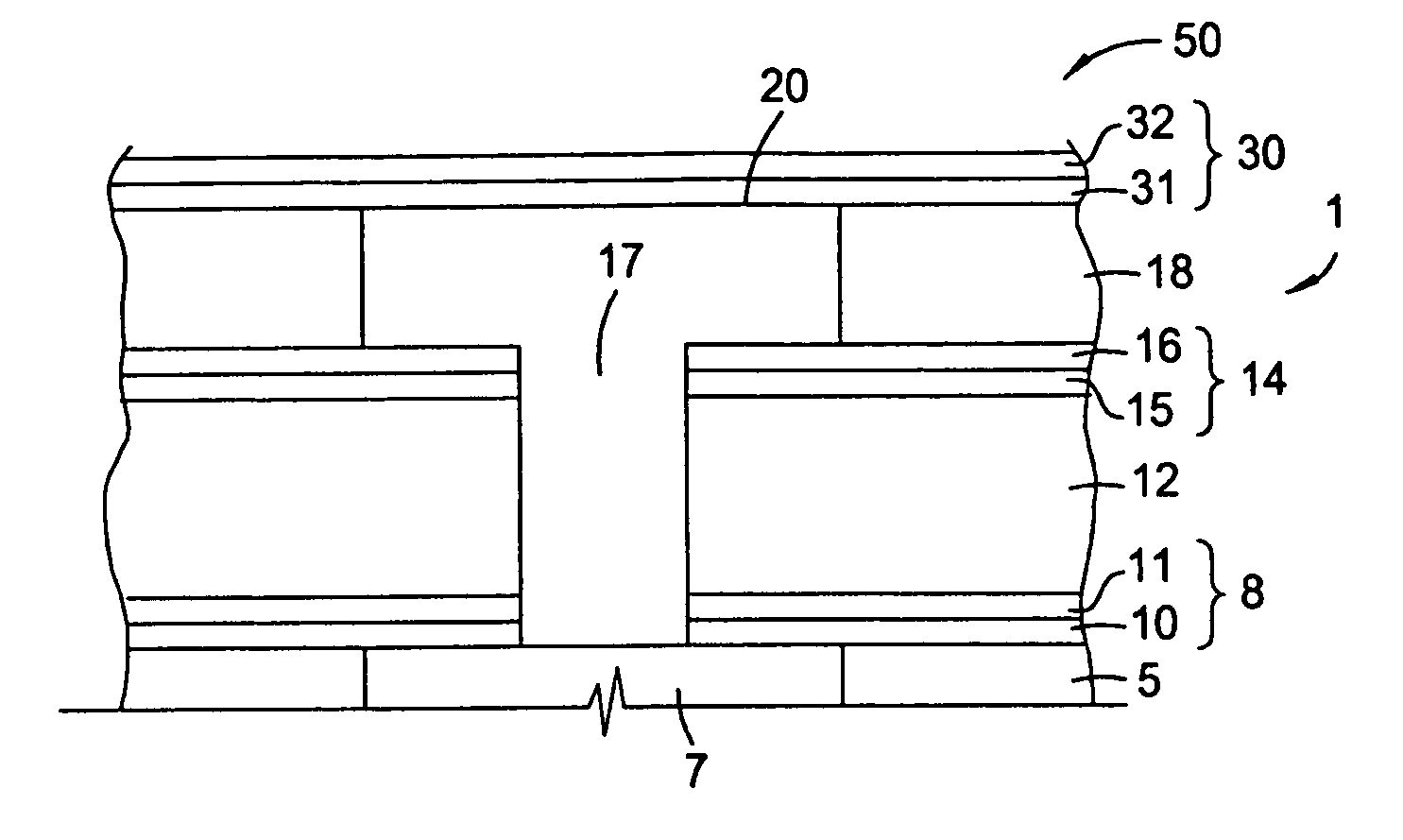
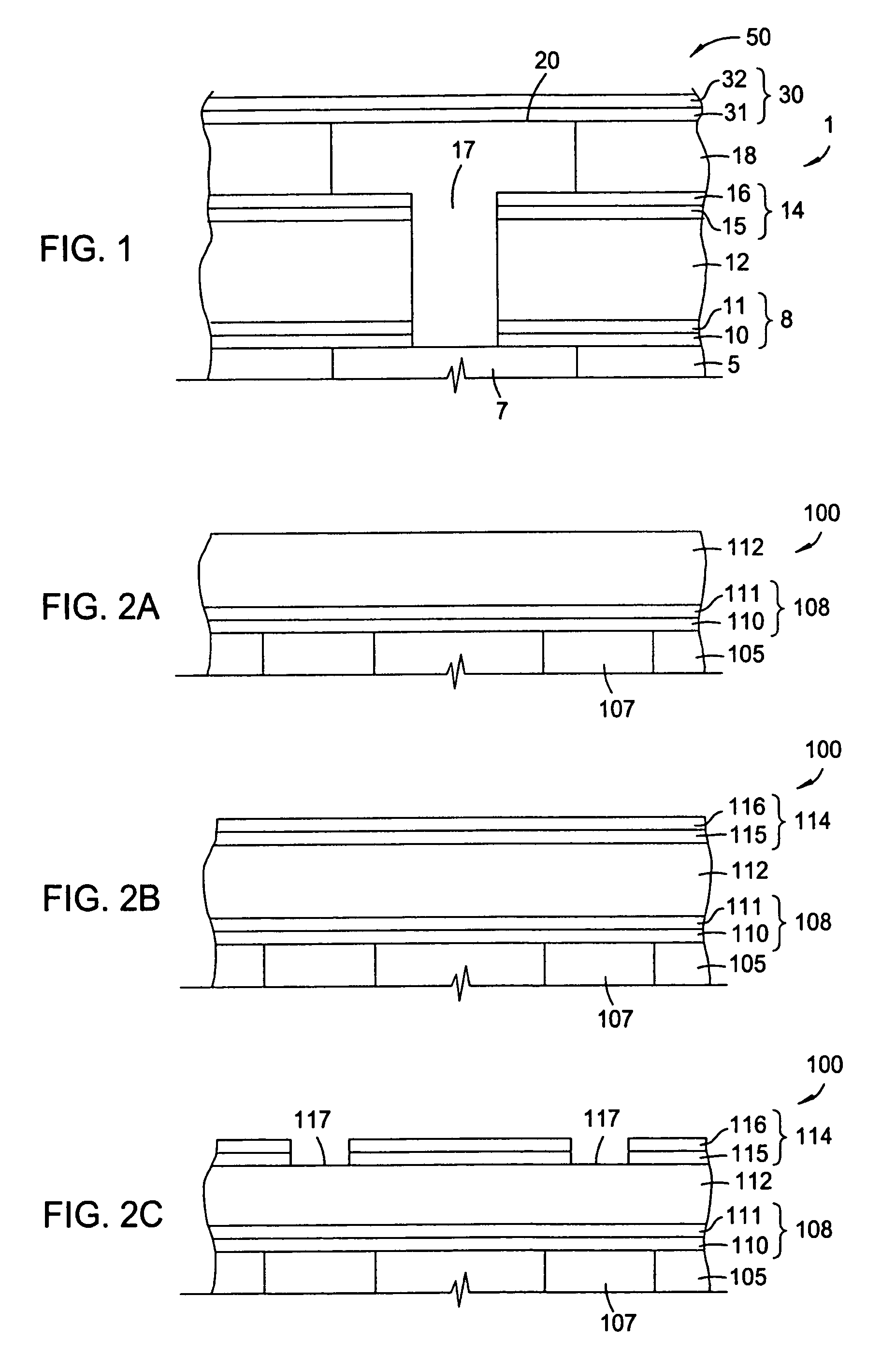
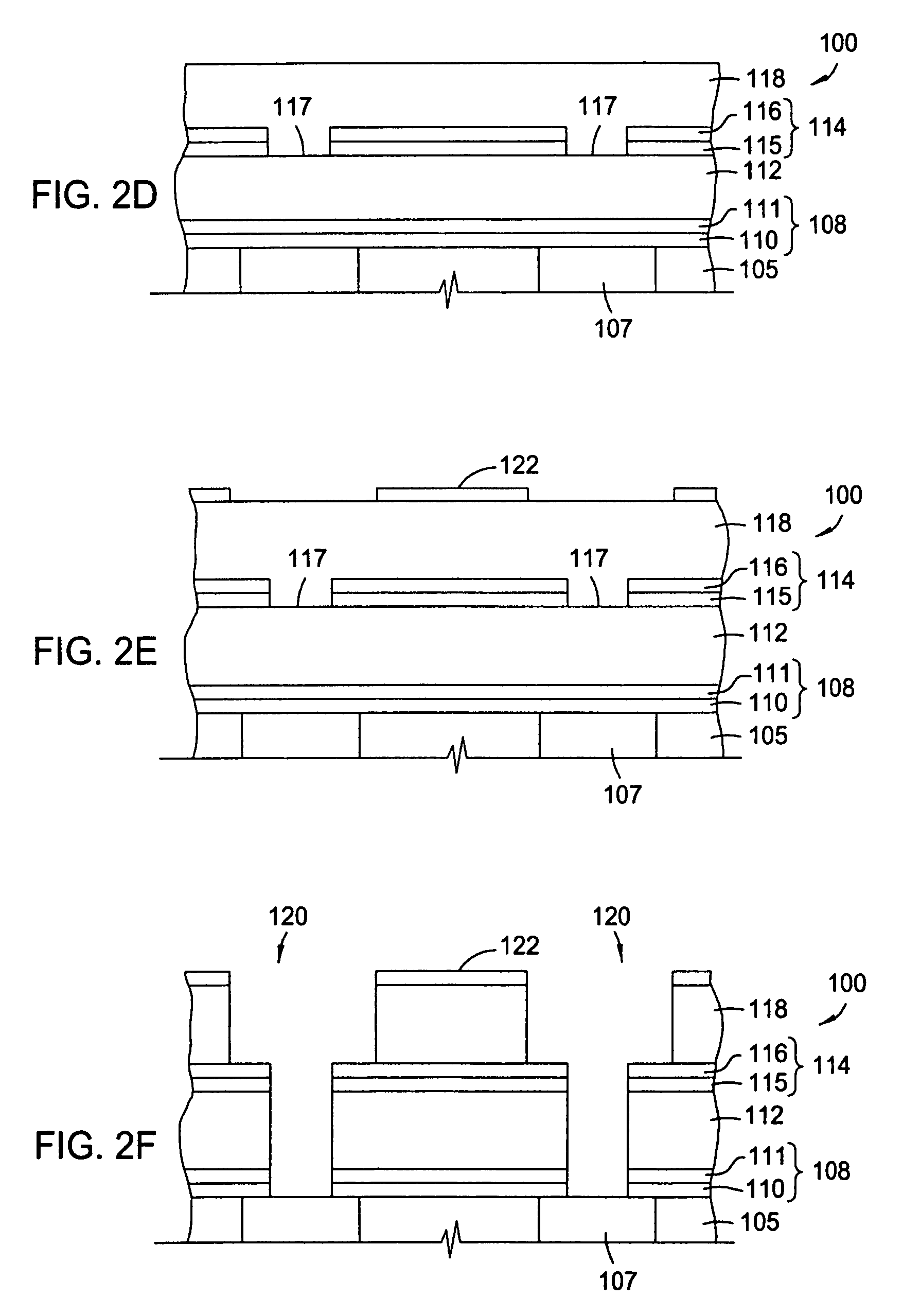
[0026]Aspects of the invention described herein refer to a method and apparatus for depositing a bilayer of silicon carbide containing materials having a low dielectric constant. The silicon carbide barrier layers include nitrogen doped silicon carbide, oxygen-doped silicon carbide, and silicon carbide deposited from aryl containing organosilicon ...


PUM

PropertyMeasurementUnit
dielectric constantaaaaaaaaaa
feature sizesaaaaaaaaaa

Abstract

Methods and apparatus are provided for processing a substrate with a bilayer barrier layer. In one aspect, the invention provides a method for processing a substrate including depositing a nitrogen containing barrier layer on a substrate surface and then depositing a nitrogen free barrier layer thereon. The barrier layer may be deposited over dielectric materials, conductive materials, or both. The bilayer barrier layer may also be used as an etch stop, an anti-reflective coating, or a passivation layer.

Description

CROSS-REFERENCE TO RELATED APPLICATIONS[0001]This application is a continuation-in-part of U.S. patent application Ser. No. 10 / 247,404, filed Sep. 19, 2002, now U.S. Pat. No. 6,838,393 which patent application claims benefit of U.S. Provisional Patent Application Ser. No. 60 / 397,184, filed Jul. 19, 2002, and is a continuation-in-part of U.S. patent application Ser. No. 10 / 196,498, filed Jul. 15, 2002, now U.S. Pat. No. 6,890,850 which patent application claims benefit of U.S. Provisional Patent Application Ser. No. 60 / 340,615, filed Dec. 14, 2001.BACKGROUND OF THE DISCLOSURE[0002]1. Field of the Invention[0003]2. Description of the Related Art[0004]Semiconductor device geometries have dramatically decreased in size since such devices were first introduced several decades ago. Since then, integrated circuits have generally followed the two year / half-size rule (often called Moore's Law), which means that the number of devices that will fit on a chip doubles every two years. Today's fa...

Claims


Application Information

Patent Timeline
Patent Type & Authority Patents(United States)
IPC IPC(8): H01L21/31C23C16/30C23C16/40C23C16/56H01L21/311H01L21/312H01L21/316H01L21/768
CPCC23C16/30H01L21/76834C23C16/56H01L21/02126H01L21/02167H01L21/022H01L21/02211H01L21/02274H01L21/02315H01L21/0234H01L21/02348H01L21/02351H01L21/3122H01L21/31633H01L21/7681H01L21/76825H01L21/76826H01L21/76828H01L21/76829H01L21/76832C23C16/401H01L21/31138H01L21/31144H01L21/312H01L21/3127H01L21/76807
Inventor LEE, ALBERTLAKSHMANAN, ANNAMALAIKIM, BOK HOENXIA, LI-QUNSHEK LE, MEI-YEE
Owner APPLIED MATERIALS INC
Why Eureka
Try Eureka