

Light emitting device
a light emitting device and light technology, applied in the direction of discharge tube luminescent screen, discharge tube/lamp details, luminescent composition, etc., can solve the problems of insatisfactory light emitting device of the prior art, decrease in relative luminance, and difficulty in satisfactorily suppressing the variation of chromaticity of light emitting device, etc., to achieve less variation in color tone, high luminance, and efficient excitation
- Summary
- Abstract
- Description
- Claims
- Application Information
AI Technical Summary
Benefits of technology
Problems solved by technology
Method used
Image

Examples
embodiment 1
[0107]The light emitting device according to the first embodiment of the present invention is constituted by the combination of:
[0108](1) a semiconductor light emitting element that emits light of a wavelength in ultraviolet region; and
[0109](2) a fluorescent substance including at least one kind of fluorescent substance (first fluorescent substance) that is excited by ultraviolet rays emitted by the light emitting element and has an emission spectrum having two peaks that are complementary colors of each other,
[0110]so as to provide the light emitted by the fluorescent substance to the outside.
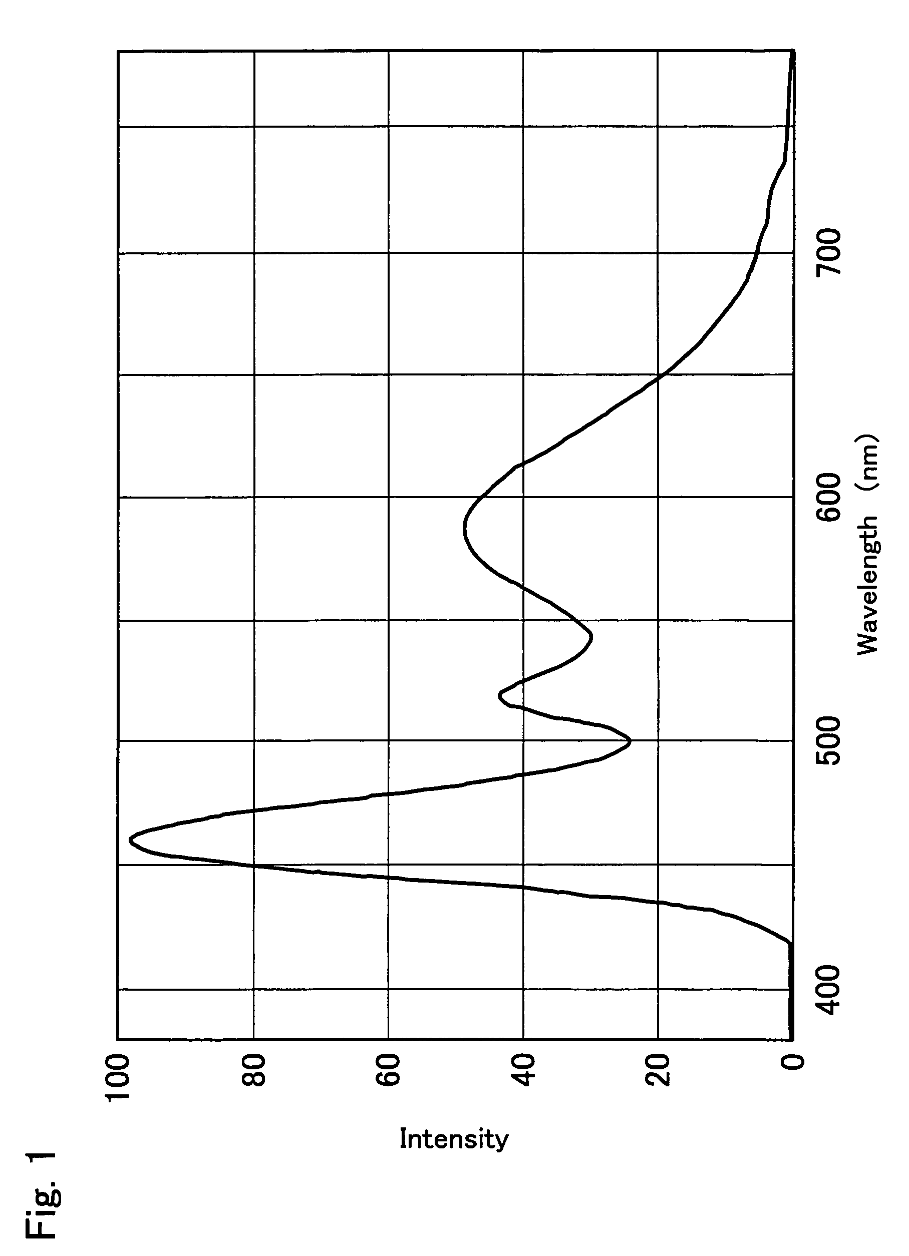
[0111]The light emitting device of the first embodiment having such a constitution as described above is hardly affected by the variability in the emission wavelength of the light emitting element as will be explained later, and the color of the emitted light is determined only by the emission spectrum of the fluorescent substance. Accordingly, such effects can be achieved as less variability...
embodiment 2
[0172]The light emitting device according to the second embodiment of the present invention will now be described below.
[0173]The light emitting device of the second embodiment is constituted in the same manner as in the first embodiment, except for using the fluorescent substance that is different from that of the first embodiment.
[0174]The light emitting device of the second embodiment emits light with less color deviation by taking advantage of the fact that the bandwidth of blurred light emitted by the fluorescent substance upon excitation by the light emitting element is less than the bandwidth of blurred light emitted by the light emitting element
[0175]While the semiconductor light emitting element is formed by the MOCVD or other process, some variability occur even among chips that are produced from a same wafer. As a result, a light emitting device that outputs the light emitted by the semiconductor light emitting element tends to produce very large variability. The light em...
example 1
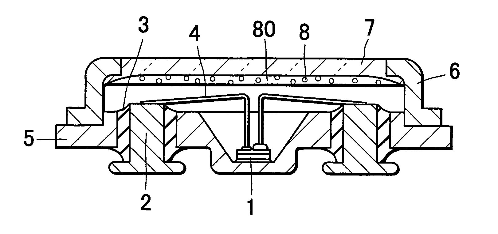
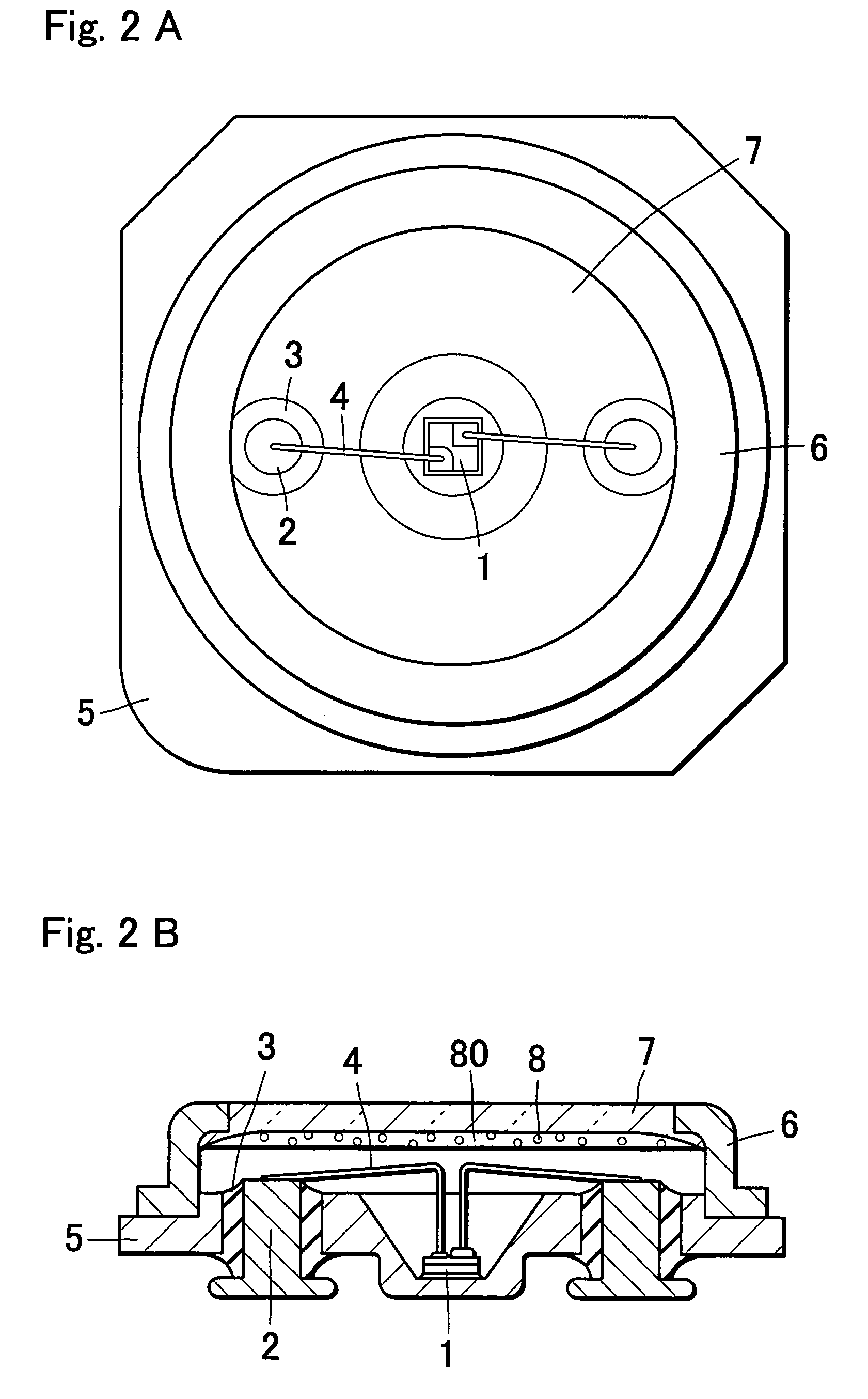
[0269]In Example 1, a surface-mounted light emitting device as shown in FIG. 2 is produced. The LED chip 1 has a light emitting layer that is constituted from a nitride semiconductor made of InAlGaN semiconductor having an emission peak at 375 nm in the ultraviolet region. The LED chip 1 is made by flowing TMG (trimethyl gallium) gas, TMI (trimethyl indium) gas, nitrogen gas and dopant gas together with a carrier gas onto a sapphire substrate that has been washed, so as to form a nitride semiconductor film by MOCVD process. At this time, layers of n-type nitride semiconductor and p-type nitride semiconductor are formed by switching the dopant gas between SiH4 and Cp2Mg.
[0270]The LED chip 1 is made in multiple quantum well structure having such a constitution as five sets of layers are stacked on the sapphire substrate, one set consisting of an n-type GaN layer made of an undoped nitride semiconductor, a GaN layer serving as n-type contact layer for forming an Si-doped n-type electro...
PUM
 Abstract
Description
Claims
Application Information