

Mechanical enhancement of dense and porous organosilicate materials by UV exposure
a technology of organosilicate materials and mechanical enhancement, which is applied in the direction of coatings, chemical vapor deposition coatings, coatings, etc., can solve the problems of only being subjected to processing temperatures, metal lines cannot be used for certain porous low dielectric compositions, and their performance deterioration, so as to improve modulus and hardness, influence the magnitude of the change in film properties, and reduce the effect of dielectric constan
- Summary
- Abstract
- Description
- Claims
- Application Information
AI Technical Summary
Benefits of technology
Problems solved by technology
Method used
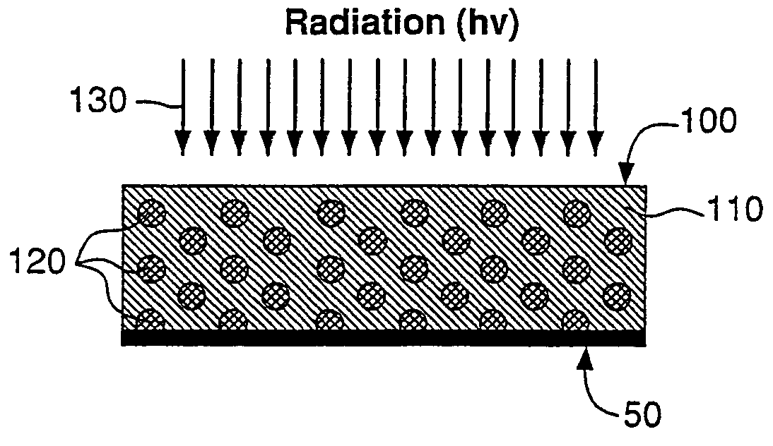
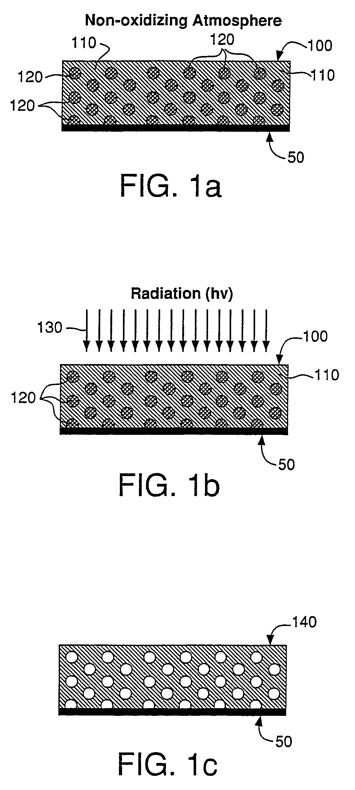
Image

Examples
example 1
Formation of a Dense OSG Film Using Diethoxymethylsilane (DEMS) and Triethoxysilane (TES)
[0072]An organosilicate glass film was formed onto a silicon wafer via plasma enhanced chemical vapor deposition (PECVD) of the structure-former precursors DEMS (773 mg / min) and TES (773 mg / min) using CO2 as the carrier gas at a flow rate of 500 sccm. The deposition was performed at 6 torr, 600 W plasma power, and 400 milli-inch (mils) spacing between the top electrode and silicon wafer substrate. The wafer temperature during deposition was maintained at 300° C. The deposition rate of the film was 540 nm / min.
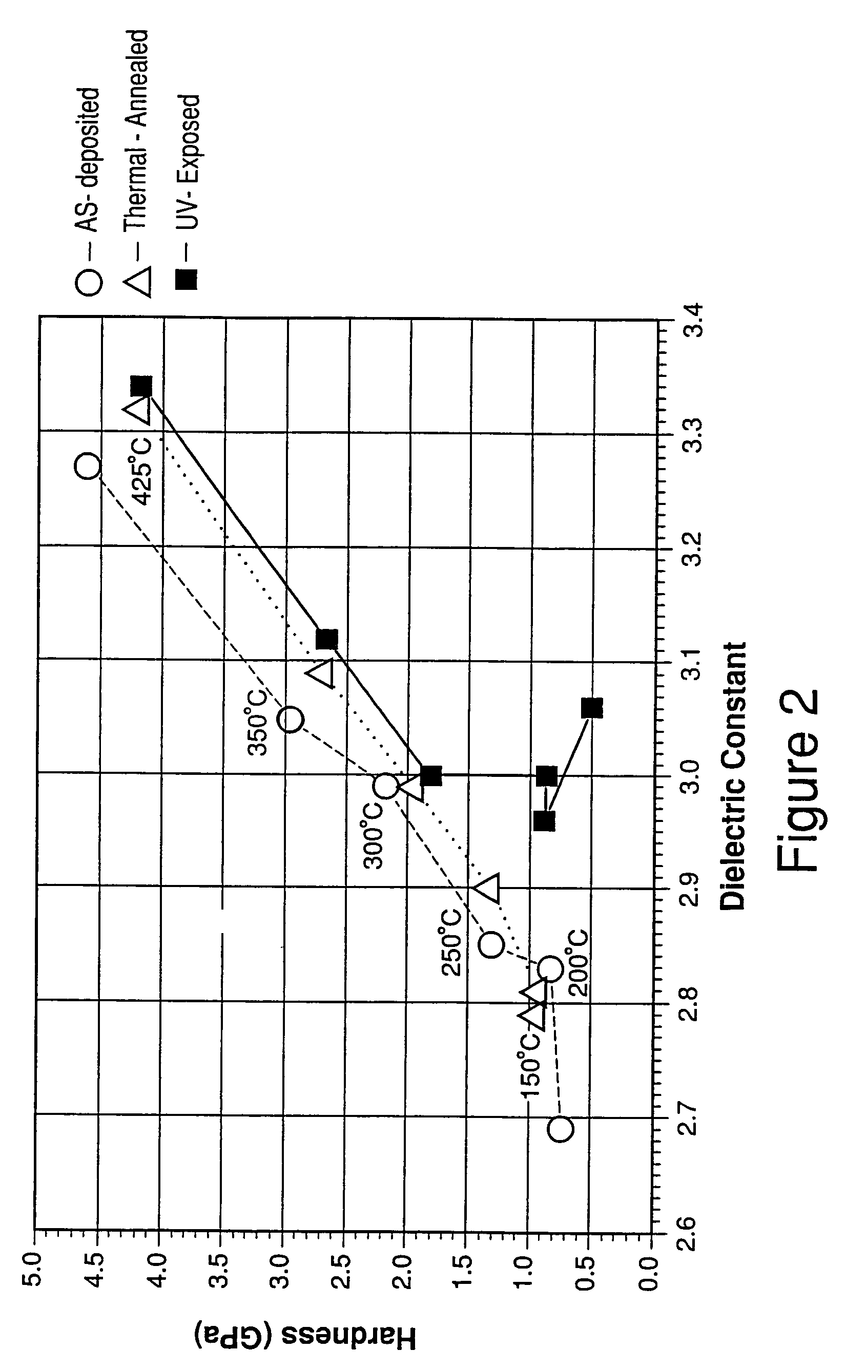
[0073]The properties of the OSG film after deposition (example 1a), after thermal anneal (example 1b), and after exposure to a UV light source (example 1c) are provided in Table I. As Table I illustrates, films 1b and 1c, which were thermally annealed and exposed to UV light respectively, exhibited a slight decrease in dielectric constant relative to example la or the as-deposited film. Howe...
example 2
Formation of a Dense OSG Films Using 1,3-dimethyl-1,3-diethoxy-disiloxane(MEDS)
[0074]An organosilicate glass film was formed onto silicon wafer via PECVD of 700 mg / min of the structure-former precursor MEDS and CO2 as the carrier gas at a flow rate of 250 sccm. The deposition was performed at 6 torr, 600 W plasma power, and 350 mils spacing. The wafer temperature during deposition was maintained at 250° C. The deposition rate of the film was 1330 nm / minute.
[0075]The properties (i.e., thickness, refractive index, dielectric constant, and hardness) of the OSG film after deposition (example 2a), after thermal anneal (example 2b), and after exposure to a UV light source (example 2c) are provided in Table I. As Table I illustrates, both films 2b and 2c, which were thermally annealed and exposed to UV light respectively, exhibited a slight increase in dielectric constant relative to film 2a or the as-deposited film. However, example film 2c exhibited a significant increase, or approximate...
example 3
Formation of a Dense OSG Films Using Trimethylsilane (3MS)
[0076]An organosilicate glass film was formed onto silicon wafer via PECVD of 540 sccm of the structure-former precursor 3MS and a flow rate of oxygen of 90 sccm. The deposition was performed at 4 torr, 600 W plasma power, and 260 mils spacing. The wafer temperature during deposition was maintained at 350° C. The deposition rate of the film was 815 nm / minute.
[0077]The properties (i.e., thickness, refractive index, dielectric constant, and hardness) of the OSG film after deposition (example 3a) and after exposure to a UV light source (example 3b) are provided in Table I. As Table I illustrates, the exposure of film 3b to UV light lowered its dielectric constant by 0.09 or 4% and increased its hardness by 0.59 GPa or 47% relative to example 3a or the as-deposited film. Thus, UV exposure provides a significant improvement in the mechanical properties and of the OSG glass film relative to thermal post-treatment using milder proce...
PUM
| Property | Measurement | Unit |
|---|---|---|
| Temperature | aaaaa | aaaaa |
| Temperature | aaaaa | aaaaa |
| Temperature | aaaaa | aaaaa |
Abstract
Description
Claims
Application Information