Lightshield architecture for interline transfer image sensors

a technology of image sensor and light shield, which is applied in the direction of semiconductor/solid-state device details, radiation control devices, solid-state devices, etc., can solve the problems of limiting the frame rate of these sensors, affecting the performance of the device, and unable to use aluminum as a lightshield material in this approach, so as to improve the performance of the image sensor

Active Publication Date: 2006-09-05
SEMICON COMPONENTS IND LLC
View PDF21 Cites 19 Cited by
  • Summary
  • Abstract
  • Description
  • Claims
  • Application Information

AI Technical Summary

Benefits of technology

[0012]This present invention provides an architecture which connects a refractory metal lightshield (such as provided by a tungsten film) to a polysilicon gate electrode without the need for barrier layers and without degradation of the image due to interaction at high temperature between the refractory lightshield and the polysilicon gate electrode. In addition this invention incorporates the reflow or anneal of a doped silicon dioxide film for improved image sensor performance.

Problems solved by technology

Such exposure will produce spurious signals in the detected image, thus degrading the performance of the device.
In large-area interline CCD devices, the high resistance of doped polysilicon electrodes combined with the large capacitance of the shift register limits the frame rate for these sensors.
Aluminum as a lightshield material cannot be used in this approach because aluminum melts at temperatures below the reflow annealing temperature.
This polysilicon layer also increases the topography of the device which may cause difficulties in depositing and patterning of later layers.

Method used


Image

  • Lightshield architecture for interline transfer image sensors
  • Lightshield architecture for interline transfer image sensors
  • Lightshield architecture for interline transfer image sensors

Examples


Embodiment Construction

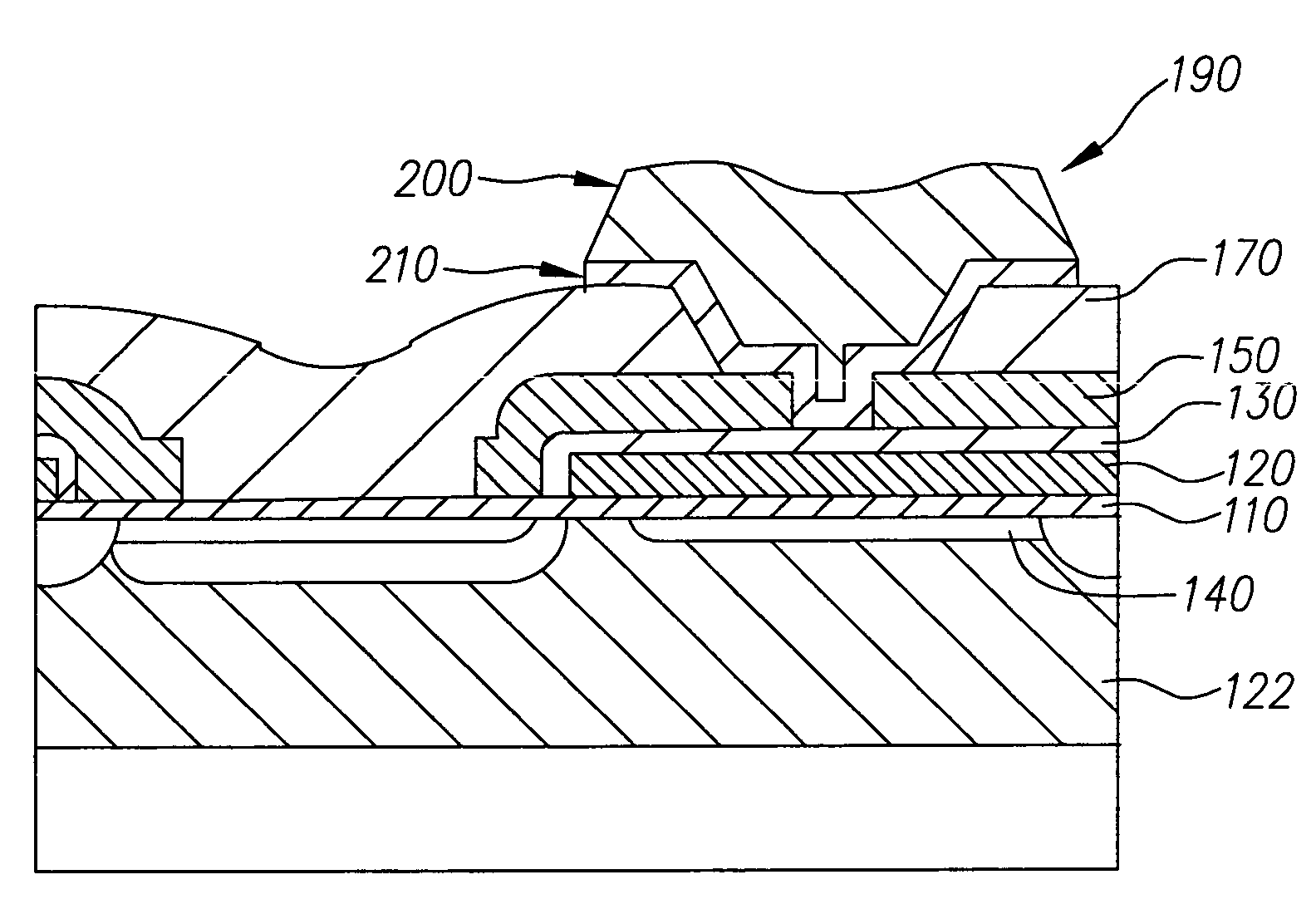
[0028]Referring to FIG. 4, there is shown the cross-section of an interline transfer pixel of the image sensor 100 of the present invention after the silicon doping layers have been formed, the gate dielectric 110 and polysilicon gate electrode 120 have been deposited and patterned, and a silicon dioxide isolation layer 130 has been grown on the polysilicon gate 120. Silicon substrate dopant regions 122, gate dielectric 110, and gate electrodes 120 form a portion of the essential elements for the interline transfer pixel as described hereinabove. In addition to those elements, a plurality of photodiodes or photosensitive areas 124 (only one is shown in FIG. 4) receive incident light that is converted into charge that is eventually transferred to the vertical CCD 140. Typically the vertical shift register portion 140 of an interline imager is constructed with many polysilicon gate electrodes 120 to enable transfer of photo-generated charge by a charge-coupled device (CCD) structure. ...


PUM


Abstract

An interline transfer type image sensing device that can be operated at high speed and with low image smear is described. The device incorporates a refractory metal layer which is used for both a light shield over the vertical charge transfer region and as a wiring layer for low resistance strapping of poly crystalline silicon (polysilicon) gate electrodes for the vertical charge transfer region. Plugs provided by a separate metallization layer connect the refractory light shield to the polysilicon gate electrode. These plugs allow high temperature processing after refractory light shield patterning for improved sensor performance without degradation of the polysilicon gate electrode or the refractory lightshield layer.

Description

FIELD OF THE INVENTION[0001]This invention relates to interlined image sensing devices and, more particularly, to such interlined image sensing devices having a plug disposed through the lightshield and insulator for directly connecting the gate electrode and lightshield for improving sensor performance.BACKGROUND OF THE INVENTION[0002]Interline transfer architecture for solid-state image sensors is well known in the prior art. Examples of such prior art image sensors include U.S. Pat. No. 4,521,797 by Oda, et al., U.S. Pat. No. 5,084,749 by Losee et al, and U.S. Pat. No. 5,235,198 by Stevens, et al., and U.S. Pat. No. 4,527,182 by Ishihara, et al. In interline transfer devices, an array of photodetectors, such as photodiodes or photocapacitors collect and store photo-generated charge. A transfer gate associated with each photodiode enables the photo-generated charge to be transferred to a vertical shift register. This transfer typically occurs at the end of the image capture period...

Claims


Application Information

Patent Timeline
Patent Type & Authority Patents(United States)
IPC IPC(8): H01L31/062H01L27/14H01L31/00H01L31/0232H01L31/113H01L27/146H01L27/148H01L31/075
CPCH01L27/14623H01L27/14685H01L27/14812H01L27/14837H01L27/14687H01L27/14843Y02E10/548
Inventor NICHOLS, DAVID N.LOSEE, DAVID L.PARKS, CHRISTOPHER
Owner SEMICON COMPONENTS IND LLC
Why Eureka
Try Eureka