System and method for improving testability independent of architecture

a testability and architecture technology, applied in the field of testability analysis systems and methods, design of testability systems and methods, can solve the problems of more large-scale, more time is required to design a test pattern for testing the integrated circuit, and the required test design time exceeds the time to design the integrated circui

Inactive Publication Date: 2006-09-05
RICOH KK
View PDF11 Cites 10 Cited by
  • Summary
  • Abstract
  • Description
  • Claims
  • Application Information

AI Technical Summary

Benefits of technology

[0014]It is a general object of the present invention to provide a testability analysis system and metho

Problems solved by technology

As an integrated circuit becomes more large-scaled and performs more complicated operations, more time is required to design a test pattern for testing the integrated circuit.
In some cases, the required test design time exceeds time to design the integrated circuit.
Japanese Laid-Open Patent Application No. 05-241882, and Japanese Patent No. 2711492) However, the signature analysis has a problem in that when an X (an unstable signal condition) is propagated to the multi-input LFSR, the reference value, which is called the signature, is collapsed.
Here, the fault coverage in the LogicBIST decreases mainly because of the difficulty of detecting faults by the random pattern test that the PRPG in the Scan-Based LogicBIST executes.
According to such a conventional LogicBIST insertion flow, there arise some problems with respect to the controllability and the observability.
First,

Method used


Image

  • System and method for improving testability independent of architecture
  • System and method for improving testability independent of architecture
  • System and method for improving testability independent of architecture

Examples


first embodiment

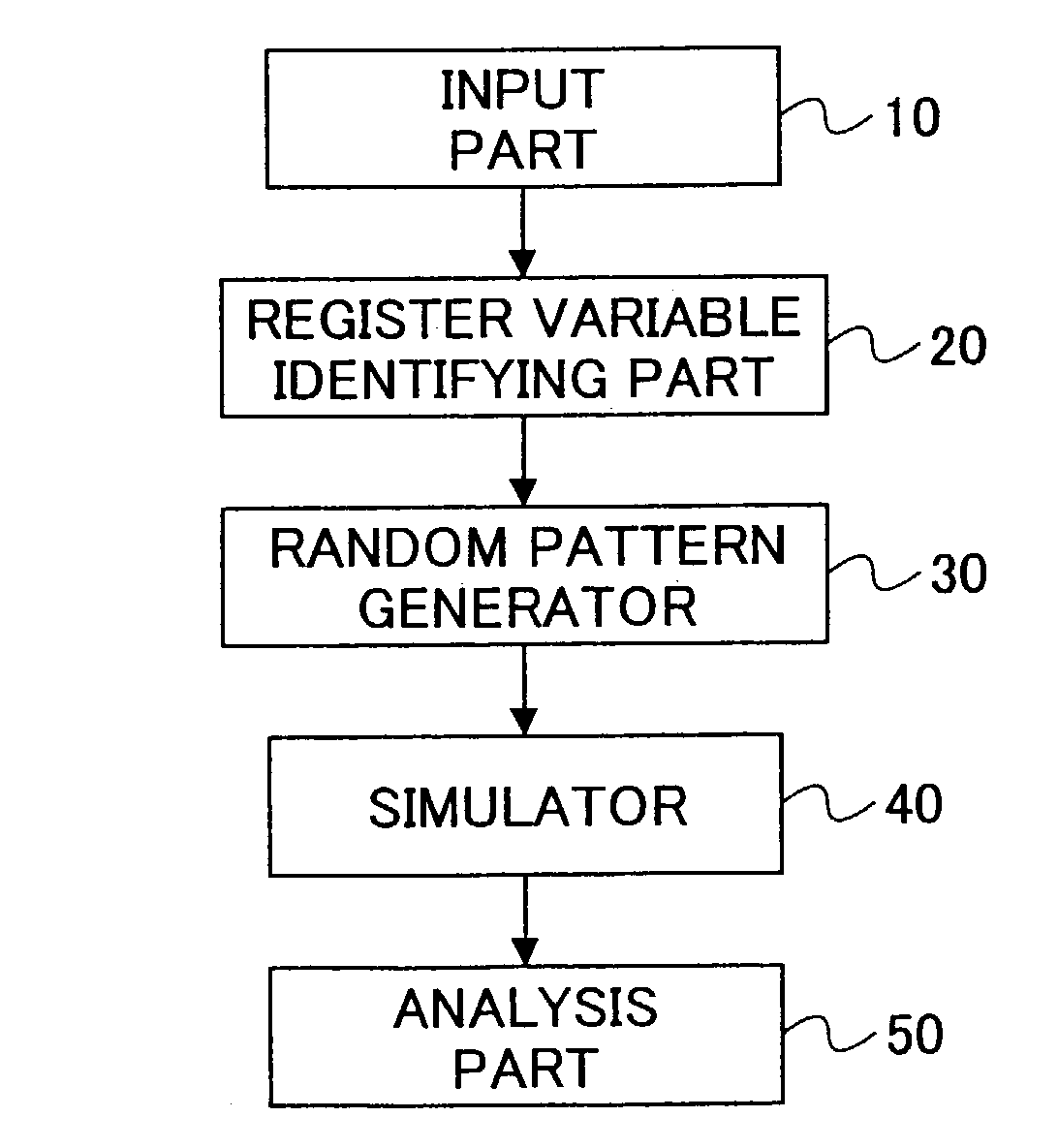
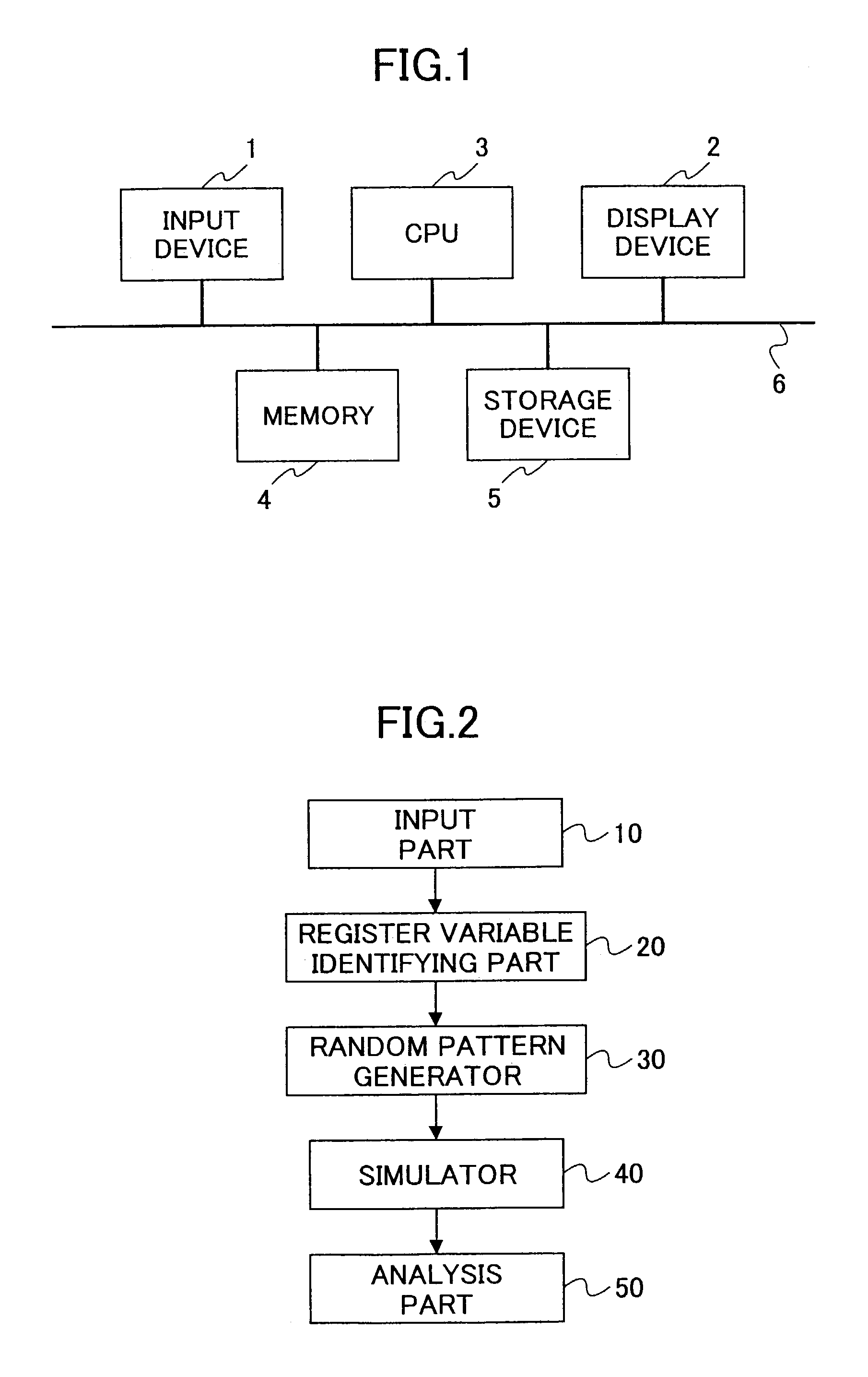
[0043]FIG. 2 is a block diagram illustrating a functional structure of a testability analysis system according to the present invention.

[0044]In FIG. 2, a function of the first embodiment comprises an input part 10, a register variable identifying part 20, a random pattern generator 30, a simulator 40, and an analysis part 50.

[0045]The input part 10 reads a hardware functional description independent of architecture from the input device 1 and temporarily saves the read hardware functional description in the storage device 5 for a later process. Here, the hardware functional description independent of architecture is written in an IEEE standard description language such as VHDL (Very high speed IC Hardware Description Language), HDL (Hardware Description Language), and Verilog-HDL. It is noted that the input part 10 may be provided to extract a hardware functional description saved in the storage device 5 in advance.

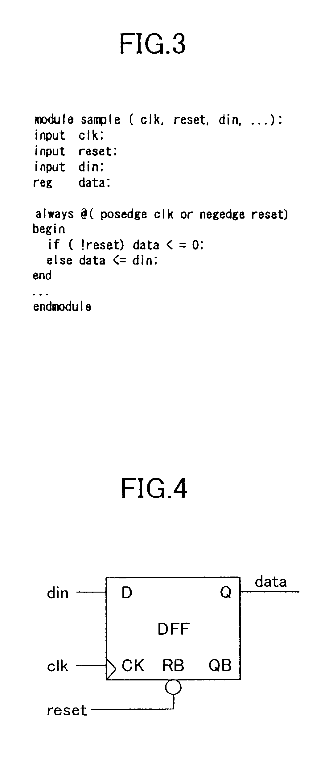
[0046]The register variable identifying part 20 identifies register...

second embodiment

[0067]A testability analysis system and a design for testability system according to the present invention are provided to give constraints for a LogicBIST execution before random patterns are applied and forced. For example, when a test is conducted by a scan path, it is necessary to turn off an asynchronous reset signal so that the scan operation cannot be collapsed.

[0068]If such constraints can be appropriately set before the random patterns are applied and forced, it is possible to realize a simulation for a hardware functional description independent of architecture wherein the random patterns are applied and forced in a similar state in which LogicBIST is operated in a netlist being at the gate level.

[0069]It is noted that the LogicBIST is used together with a boundary scan testing mechanism proposed by an organization JTAG (Joint Test Action Group) whose members are semiconductor manufacturers in Europe and the U.S. In this case, it is sufficient to provide a sequence to be s...

third embodiment

[0085]As a result, in the third embodiment, it is possible to examine the testability regarding a LogicBIST testing mode when the logic synthesis is operated and to add an alternate path and a testing circuit to a net whose toggle rates and simulation events are not sufficient. Thus, it is possible to avoid a circuit timing loss caused by an addition of a testing circuit to a netlist being at the gate level as in a conventional method.

[0086]The present invention is not limited to the above-mentioned embodiments. Programs to execute individual features of the above-mentioned embodiments may be written into a recording medium such as a CD-ROM so that a CPU in a computer can read and execute the saved programs in the recording medium by saving the programs into a memory or a storage device by means of an equipped medium driving device such as a CD-ROM drive. Also in the above method, the present invention is achieved.

[0087]Also, if the above-programs are saved in a ROM (Read Only Memor...


PUM


Abstract

A testability analysis system analyzes testability by evaluating controllability and observability at the level of a hardware functional description independent of architecture. The testability analysis system comprises: an input part inputting functional description data to define a hardware function; a register variable identifying part identifying register variables whereby memory elements such as a flip-flop in said functional description data are inferred; a random pattern generator applying random patterns to the register variable identified by said register variable identifying part; a simulator conducting a simulation on an event caused by applying the random patterns; and an analysis part analyzing a cause of decrease of a fault coverage by LogicBIST, which is mainly caused by the difficulty of detecting faults by the random pattern test that PRPG (Pseudo Random Pattern Generator) of the Scan-Based LogicBIST executes, based upon toggle rates and simulation events of variables (such as net and bus) in said functional description data in accordance with a result of said simulation.

Description

BACKGROUND OF THE INVENTION[0001]1. Field of the Invention[0002]The present invention generally relates to testability analysis systems and methods, designs for testability system and method and, more particularly, to a testability analysis system and method, and a design for testability system and method that can analyze controllability and observability with a logic built-in self testing mechanism at the level of a hardware functional description independent of architecture for a large scale integrated circuit.[0003]2. Description of the Related Art[0004]As an integrated circuit becomes more large-scaled and performs more complicated operations, more time is required to design a test pattern for testing the integrated circuit. In some cases, the required test design time exceeds time to design the integrated circuit.[0005]Accordingly, it is indispensable to prepare a DFT (Design For Testability) whereby a large-scale integrated circuit is provided with some measures for reducing s...

Claims


Application Information

Patent Timeline
IPC IPC(8): G06F17/50G01R31/28G01R31/3183G11C29/54H01L21/82H04L1/24
CPCG01R31/318342G01R31/318385H04L1/244G11C29/56004G11C29/54
Inventor YAMADA, TAKAMITSU
Owner RICOH KK
Why Eureka
Try Eureka