

Method for forming a wiring of a semiconductor device, method for forming a metal layer of a semiconductor device and apparatus for performing the same
a technology of semiconductor devices and metal layers, applied in the field of semiconductor devices, can solve the problems of more difficult wiring, aluminum ring defects may be generated along the interface between grains of aluminum, and the titanium nitride layer is not well suited as a metal barrier layer, etc., and achieves the effect of improving the step coverage and simple processing parameters
- Summary
- Abstract
- Description
- Claims
- Application Information
AI Technical Summary
Benefits of technology
Problems solved by technology
Method used
Image

Examples
embodiment 1
[0084]FIGS. 3A to 3F are cross sectional views illustrating a method for forming a wiring according to a first embodiment of the present invention.
[0085]Referring to FIG. 3A, a first wiring 32 is formed on a substrate 30. The first wiring 32 may include polysilicon, titanium, tantalum, aluminum, copper, tungsten, novel metal, metal nitride or a mixture thereof. Examples of the novel metal may include Ru, Pt or Ir. Examples of the metal nitride may include titanium nitride, tantalum nitride or tungsten nitride. Additionally, the substrate 30 may be cleaned using a plasma before the formation of the first wiring 32.
[0086]Referring to FIG. 3B, an insulating layer 34 is formed on the first wiring 32. The insulating layer 34 may include oxide.
[0087]Referring to FIG. 3C, the insulating layer 34 is etched by a typical photolithography process to form an insulating layer pattern 34a having a contact hole 35.
[0088]Referring to FIG. 3D, a second wiring 36 is formed by an ALD process or a CVD ...
embodiment 2
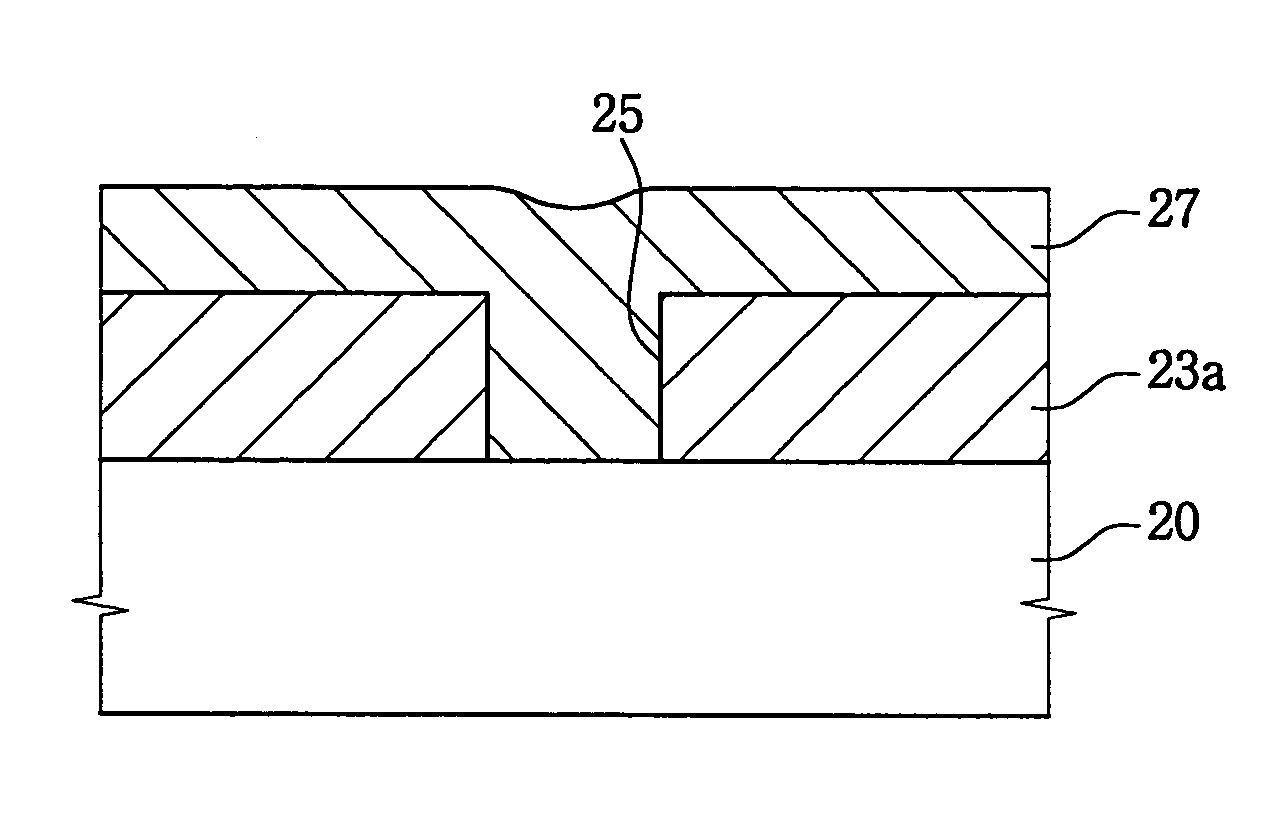
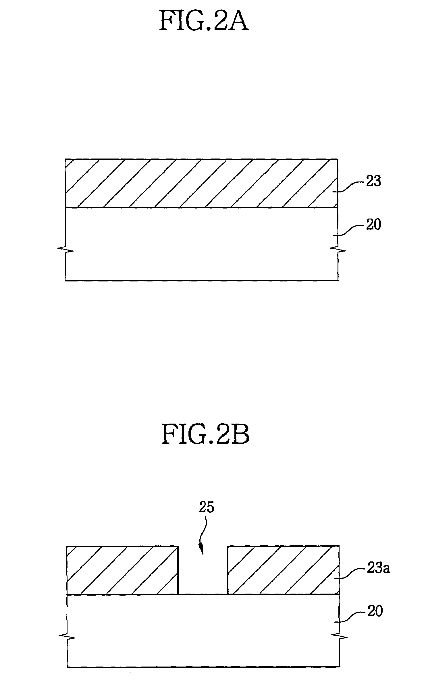
[0092]FIGS. 4A and 4B are cross sectional views illustrating a method for forming a wiring according to a second embodiment of the present invention.
[0093]Referring to FIG. 4A, a first wiring 42 is formed on a substrate 40. An insulating layer is formed on the first wiring 42. The insulating layer is etched to form an insulating layer pattern 44a having a contact hole 45.
[0094]Referring to FIG. 4B, a second wiring is formed on the insulating layer pattern 44a, and a side wall and a bottom face of the contact hole 45. The second wiring may include polysilicon, titanium, tantalum, aluminum, copper, tungsten, novel metal, metal nitride or a mixture thereof. Examples of the novel metal may include Ru, Pt or Ir. Examples of the metal nitride may include titanium nitride, tantalum nitride or tungsten nitride. The substrate 40 may be cleaned using a plasma before the formation of the second wiring.
[0095]The second wiring is removed by an etching process or a CMP process to expose an upper ...
embodiment 3
[0098]FIGS. 5A to 5C are cross sectional views illustrating a method for forming a wiring according to a third embodiment of the present invention.
[0099]Referring to FIG. 5A, a first wiring 52 is formed on a substrate 50. An insulating layer is formed on the first wiring 52. The insulating layer is etched to form an insulating layer pattern 54a having a contact hole 55.
[0100]Referring to FIG. 5B, a metal barrier layer 56 is formed on the insulating layer pattern 44a, and a side wall and a bottom face of the contact hole 45. In particular, a source gas including Ta(NC(Ch3)2C2H5)(N(CH3)2)3) and a reacting gas including NH3 are simultaneously introduced over the substrate 30 at a temperature of about 300° C. The NH3 gas is introduced at a flow rate of 600 sccm. A gas mixed of H2 having a flow rate of about 1,000 sccm and Ar having a flow rate of about 500 sccm is used as a purge gas. An Ar gas having a flow rate of about 100 sccm is used as a carrier gas of Ta(NC(Ch3)2C2H5)(N(CH3)2)3)....
PUM
| Property | Measurement | Unit |
|---|---|---|
| temperature | aaaaa | aaaaa |
| temperature | aaaaa | aaaaa |
| thickness | aaaaa | aaaaa |
Abstract
Description
Claims
Application Information