Semiconductor device and semiconductor device producing system

a semiconductor device and semiconductor technology, applied in the field of semiconductor device and semiconductor device producing system, can solve the problems of accumulating distortions, single crystalline semiconductor film cannot be formed, and the surface of single crystalline semiconductor film is disadvantageously affected, so as to reduce the on-current, reduce the mobility, and improve the crystallinity.

Inactive Publication Date: 2006-10-03
SEMICON ENERGY LAB CO LTD
View PDF132 Cites 45 Cited by
  • Summary
  • Abstract
  • Description
  • Claims
  • Application Information

AI Technical Summary

Benefits of technology

[0016]Recently, technologies each for forming a TFT over a substrate have been evolved significantly. The technologies have been applied to the active matrix type semiconductor display device. Especially, a TFT using a polycrystalline semiconductor film has higher field effect mobility than that of a TFT having a conventional amorphous semiconductor film. Therefore, rapid operations are possible. Thus, pixel control, which has been performed by a drive circuit provided outside of a conventional substrate, can be performed by a drive circuit over a substrate on which pixels are also provided.
[0063]Multiple laser light beams are overlapped to compensate each other for the parts with lower energy densities. Thus, crystallinity of the semiconductor film can be improved efficiently by overlapping multiple laser light beams rather than using the laser light beams separately.

Problems solved by technology

As a result, the grade changes remain on the surface of the formed single crystalline semiconductor film disadvantageously.
Furthermore, a single crystalline semiconductor film cannot be formed by using the graphoepitaxy on a large glass substrate having smaller distortion points.
Furthermore, distortions are accumulated.
Thus, an area causing defects cannot be positionally controlled so as to position in the other area than element forming areas.
Accordingly, without bonded SOI (silicon on insulator), a crystalline semiconductor film on an insulating surface cannot obtain the same quality as that of a MOS transistor provided on a single crystalline semiconductor.

Method used


Image

  • Semiconductor device and semiconductor device producing system
  • Semiconductor device and semiconductor device producing system
  • Semiconductor device and semiconductor device producing system

Examples


examples

[0182]Examples of the present invention will be described below.

first example

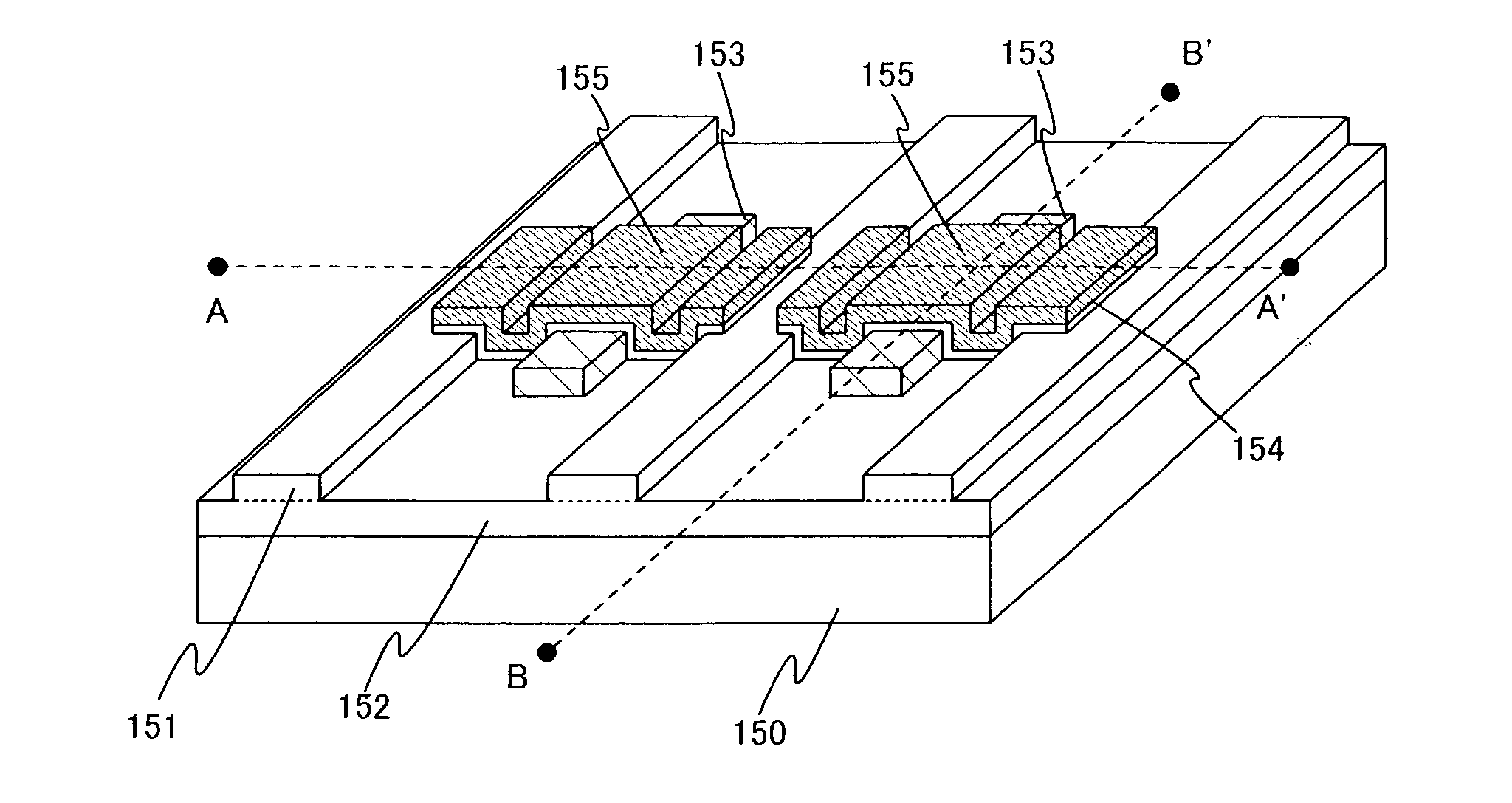
[0183]A first example is a case where a crystalline semiconductor film is formed on a primary insulating film having grade changes. Then, a TFT is produced in which a channel forming regions are provided in a crystalline semiconductor film on the projection top portion.

[0184]In FIGS. 32A to 32F, a first insulating film 9602, which is a silicon oxide nitride film of 100 nm in thickness, is formed on a glass substrate 9601. Then, a silicon nitride film is formed thereon, and second insulating films 9603 to 9607 are formed having a rectangular pattern by photo-engraving. The silicon oxide nitride film and the silicon nitride film are formed by Plasma CVD method.

[0185]After an amorphous silicon film 9608 of 150 nm in thickness is formed by Plasma CVD method, a continuous-wave laser beam is irradiated thereto for the crystallization. FIG. 34 is a top view thereof. FIG. 32A is a vertical section diagram taken at a line A–A′ in FIG. 34. Areas 9611 to 9613 indicated by one-dashed lines over...

second example

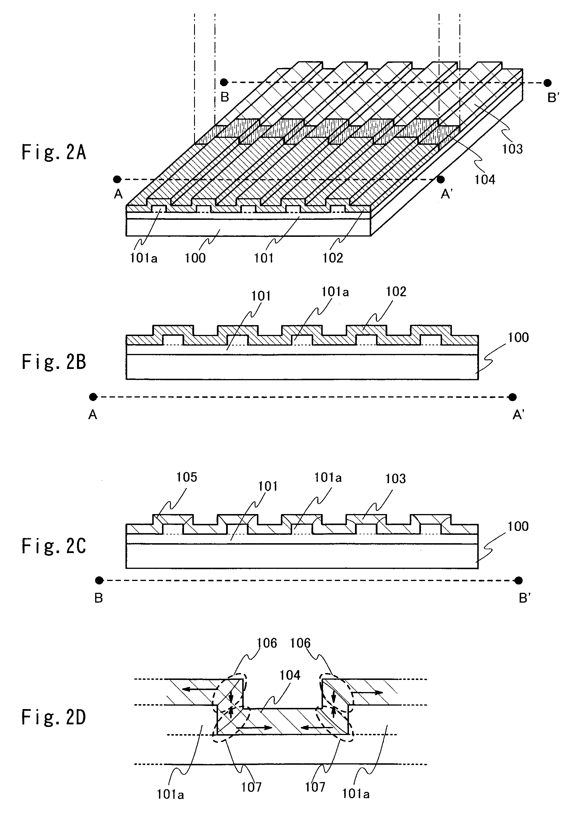
[0191]Like the first example, in order to form active layers, a laser beam may be irradiated to an amorphous semiconductor film for crystallization. However, after poly-crystallization, the laser beam may be further irradiated so as to improve the crystallinity. This two-level crystallization processing can form a crystalline semiconductor film having fewer distortions than those of the first example.

[0192]FIGS. 38A to 38C are vertical section diagrams showing the processing steps. In FIG. 38A, a first insulating film 9502, which is a silicon oxide nitride film of 100 nm in thickness, is formed on a glass substrate 9501. A silicon oxide film is formed thereon, and second insulating films 9503 to 9506 are formed having a rectangular pattern by photo-engraving. Then, an amorphous silicon film 9507 of 150 nm in thickness is formed thereon.

[0193]Ni is added to an entire surface of the amorphous semiconductor film 9507. Ni is a medium element, which can decrease a temperature for crystal...


PUM

PropertyMeasurementUnit
wave lengthaaaaaaaaaa
thicknessaaaaaaaaaa
thicknessaaaaaaaaaa

Abstract

An insulating film having depressions and projections are formed on a substrate. A semiconductor film is formed on the insulating film. Thus, for crystallization by using laser light, a part where stress concentrates is selectively formed in the semiconductor film. More specifically, stripe or rectangular depressions and projections are provided in the semiconductor film. Then, continuous-wave laser light is irradiated along the stripe depressions and projections formed in the semiconductor film or in a direction of a major axis or minor axis of the rectangle.

Description

BACKGROUND OF THE INVENTION[0001]1. Field of the Invention[0002]The present invention relates to a semiconductor device including a semiconductor film having a crystal structure and particularly to a semiconductor device including a crystalline semiconductor film raised on an insulating surface and a field-effect transistor such as a thin film transistor and / or a bipolar transistor especially. In addition, the present invention relates to a semiconductor device producing system for crystallizing a semiconductor film by using laser light and for activating a semiconductor film after ion implantation.[0003]2. Description of the Related Art[0004]A technology has been known for crystallizing an amorphous semiconductor film over a substrate of, for example, glass through laser processing. The laser processing may be a technology for re-crystallizing a damaged layer or an amorphous layer on a semiconductor substrate or a semiconductor film, a technology for crystallizing an amorphous semi...

Claims


Application Information

Patent Timeline
Patent Type & Authority Patents(United States)
IPC IPC(8): H01L31/036H01L21/84B23K26/00B23K26/03B23K26/067B23K26/08B23K26/10B23K26/42H01L21/20H01L21/77H01L29/786H01L31/00
CPCB23K26/032B23K26/0608B23K26/067B23K26/0738B23K26/0853B23K26/10B23K26/422H01L21/2026H01L29/78603H01L27/1281B23K2201/40B23K2101/40B23K26/702H01L21/02494H01L21/02686H01L21/02683H01L21/02678H01L21/02502H01L21/02488H01L21/02422H01L21/02532H01L21/02598H01L21/02672H01L21/02691H01L21/268
Inventor ISOBE, ATSUODAIRIKI, KOJISHIBATA, HIROSHIKOKUBO, CHIHOARAO, TATSUYAHAYAKAWA, MASAHIKOMIYAIRI, HIDEKAZUSHIMOMURA, AKIHISATANAKA, KOICHIROYAMAZAKI, SHUNPEIAKIBA, MAI
Owner SEMICON ENERGY LAB CO LTD
Why Eureka
Try Eureka