Luminescent apparatus and method of manufacturing the same

a technology of luminescent apparatus and manufacturing method, which is applied in the direction of discharge tube luminescnet screen, discharge tube/lamp details, organic semiconductor device, etc., can solve the problems of early deterioration of organic el film, inability to apply a uniform voltage to the anode, and thermal treatment of over 150° c. , to achieve the effect of reducing resistance value and high quality

Inactive Publication Date: 2006-10-03
SEMICON ENERGY LAB CO LTD
View PDF30 Cites 40 Cited by
  • Summary
  • Abstract
  • Description
  • Claims
  • Application Information

AI Technical Summary

Benefits of technology

[0028]In the luminescent apparatus including the above-described structures according to the present invention, the auxiliary electrode 107 functions as an electrode connected to the transparent electrode 104, which is formed of a transparent conductive film, in parallel therewith. Since the auxiliary electrode 107 is formed on the side of the seal member 106, a resistance value can be reduced to a low level without being restricted by the low thermal resistance of the organic EL film referred to in the descriptions of the related art examples. Therefore, when the present invention is put into practice, it becomes possible to apply a uniform voltage to the transparent electrode 104 and obtain an image of a high quality.

Problems solved by technology

In order to obtain a bright image when the effective emission region is narrow, it is necessary to increase an emission brightness but increasing the emission brightness results in an early deterioration of the organic EL film.
However, the structure shown in FIG. 9B has potentially a problem that the structure is incapable of applying a uniform voltage to the anode 909.
However, since the organic EL film has a low thermal resistance, a thermal treatment of over 150° C. cannot be conducted after the organic EL film has been formed.
Therefore, when an anode (transparent conductive film) is laminated on an organic EL film, a thermal treatment cannot be conducted, so that it is difficult to form an anode of a low resistance value.
There is a fear that this problem causes a decrease in the quality of an image.
As mentioned above, in a luminescent apparatus including a structure using a transparent conductive film formed after the formation of an organic EL film, it is difficult to reduce the resistance of the transparent conductive film.

Method used


Image

  • Luminescent apparatus and method of manufacturing the same
  • Luminescent apparatus and method of manufacturing the same
  • Luminescent apparatus and method of manufacturing the same

Examples


embodiment ] 2

[Embodiment]2

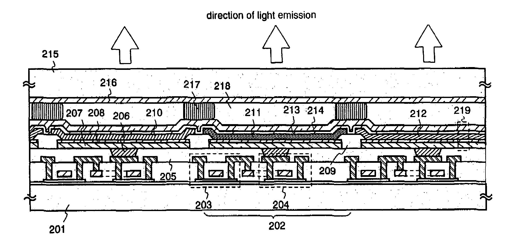
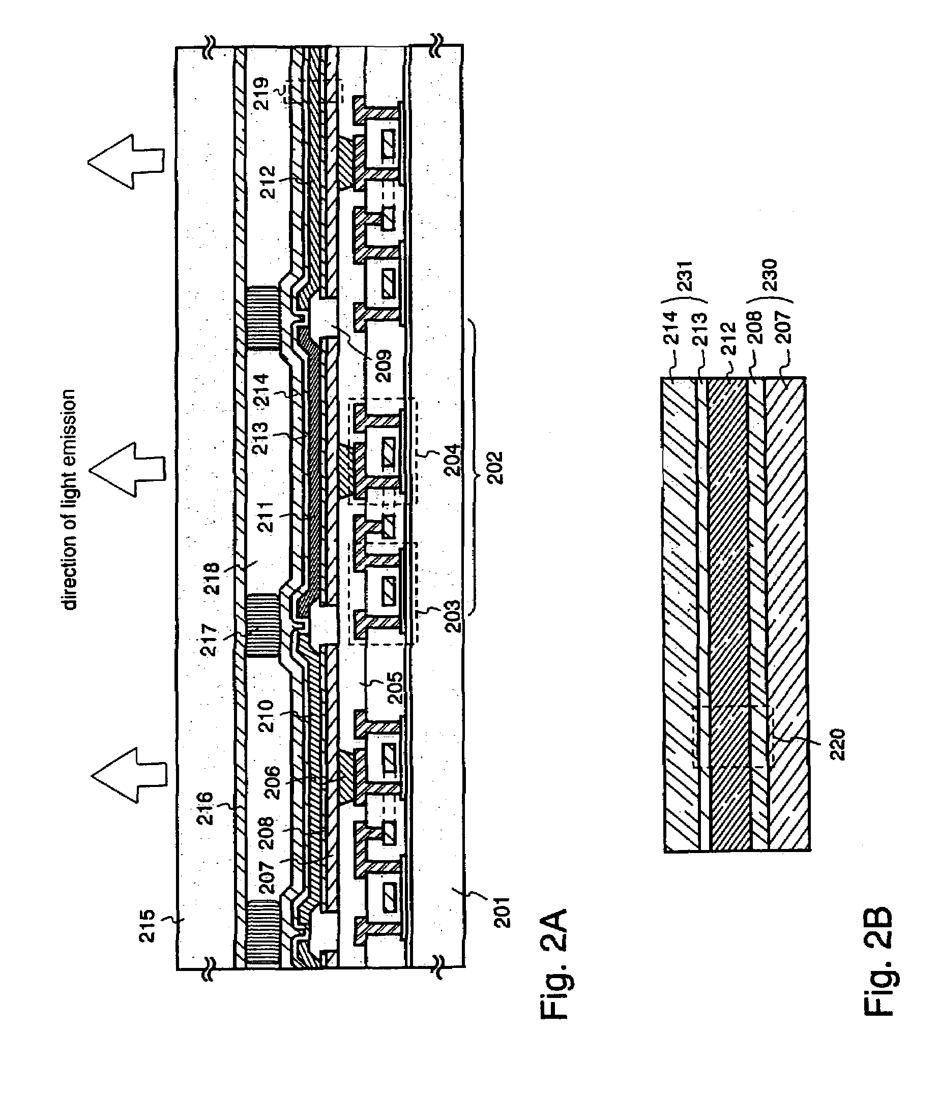
[0097]In this embodiment, an EL luminescent apparatus having pixels the structure of which is different from that of the pixels of the EL luminescent apparatus shown in FIG. 2 will be described with reference to FIG. 7. The embodiment of FIG. 7 can be manufactured, by only slightly modifying the structure of FIG. 2, and will be described with attention paid to the points of the former embodiment which are different from the corresponding points of the latter embodiment. Therefore, concerning the parts of the embodiment of FIG. 7 which are designated by reference numerals identical with those used in FIG. 2, the statement under “Description of the Preferred Embodiment” may be referred to.

[0098]In the embodiment of FIG. 7, contact holes are formed in an interlayer insulating film 205, and a pixel electrode 701 and a first transparent electrode 702 are thereafter formed in the same condition, an insulating film 703 being then formed so as to fill recessed portions due to c...

embodiment ] 3

[Embodiment]3

[0104]Although only the construction of pixels is shown in the EL luminescent apparatuses shown in the mode of embodiment and Embodiment 1, a circuit for driving the pixels may be formed in a body on the same substrate. In this case, the driving circuit can be formed of an nMOS circuit, a pMOS circuit, or a CMOS circuit. It is, of course, allowable to form the pixel portions alone of TFTs, and use an externally fixed driving circuit, typically, an IC tip-including driving circuit (TCP and COG).

[0105]In Embodiment 1, the pixel portions are formed by p-channel type TFTs only, and the number of the manufacturing steps are thereby reduced. In this case, it is also possible to form the driving circuit by a pMOS circuit, and use an IC tip-including driving circuit as a driving circuit unable to be formed by a pMOS.

[0106]The structure of this embodiment can be put into practice by freely combining the same with the structure of Embodiment 1 or 2.

embodiment ] 4

[Embodiment]4

[0107]In this embodiment, an example using an amorphous silicon film as an active layer of switching TFTs and current control TFTs formed in pixel portions is shown. An inversely staggered TFT is known as a TFT using an amorphous silicon film, and can also be used in this embodiment.

[0108]Although a step of manufacturing a TFT using an amorphous film is simple, a size of an element becomes large. In the EL luminescent apparatus according to the present invention, the size of TFT does not have influence upon the effective emission surface area. Therefore, a more inexpensive EL luminescent apparatus can be manufactured by using an amorphous silicon film as an active layer.

[0109]The structure of this embodiment can be put into practice by freely combining with any of those of Embodiments 1-3. However, when the structure of Embodiment 4 is combined with that of Embodiment 3, it is difficult to manufacture a driving circuit of a high operating speed by a TFT using an amorpho...


PUM


Abstract

The present invention provides a luminescent apparatus having a bright, high-quality image. A reflecting surface-including electrode, and an EL element formed of an organic EL layer and a transparent electrode are provided on an insulator. As shown in FIG. 1, an auxiliary electrode 107 formed of a transparent conductive film is connected to the transparent electrode via a conductor. This structure enables a resistance value of the transparent electrode 104 to be substantially lowered, and a uniform, voltage to be applied to the organic EL layer.

Description

CROSS-REFERENCE TO RELATED APPLICATION[0001]This application is a divisional application of U.S. application Ser. No. 09 / 851,656, filed on May 8, 2001 U.S. Pat. No. 6,608,449, now allowed, which claims the benefit of a foreign priority application filed in Japan on May 8, 2000 as Ser. No. 2000-135076, both of which are incorporated by reference.BACKGROUND OF THE INVENTION[0002]1. Field of the Invention[0003]This invention relates to a luminescent apparatus using a thin film made of a luminescent material, and also to an electric appliance using the luminescent apparatus as a display. An organic EL display and an organic light-emitting diode (OLED) are included in the luminescent apparatus according to the present invention.[0004]The luminescent materials which can be used for the present invention include all luminescent materials that emit light (phospholescence and / or fluorescence) via singlet excitation or triplet excitation or both thereof.[0005]2. Description of the Related Art...

Claims


Application Information

Patent Timeline
Patent Type & Authority Patents(United States)
IPC IPC(8): H01J1/62H01J63/04H01L27/32H01L51/52
CPCH01L27/3244H01L27/3276H01L51/5206H01L51/5212H01L51/5234H01L51/5237H01L27/3211H01L51/524H01L51/5284H01L2251/5315H01L27/3248H10K59/35H10K59/123H10K59/12H10K59/131H10K50/81H10K50/814H10K50/828H10K50/8423H10K50/8428H10K50/841H10K50/865H10K2102/3026
Inventor FUKUNAGA, TAKESHI
Owner SEMICON ENERGY LAB CO LTD
Why Eureka
Try Eureka