Complementary voltage controlled oscillator

a voltage control and complementary technology, applied in the field of electric oscillator circuits, can solve the problems of poor circuit performance in a wireless communication system, low frequency stability of the oscillator, and degraded oscillation performance, so as to facilitate the layout of the integrated circuit, optimize phase noise performance, and reduce the side effects of parasitic characteristics

Inactive Publication Date: 2006-10-17
NEOREACH INC
View PDF3 Cites 9 Cited by
  • Summary
  • Abstract
  • Description
  • Claims
  • Application Information

AI Technical Summary

Benefits of technology

[0013]A voltage controlled oscillator is provided according to the teachings of the present invention. The oscillator addresses and mitigates the problems explained above. High performance and low phase noise are achieved by the present circuitry structure, and in addition performance degradation is prevented with reduced passive components so as to decrease the parasitic effects present in such components. In a preferred embodiment of this invention, a complementary Colpitts (also termed C-Colpitts) oscillator topology is provided that is effectively composed primarily of two components, a complementary N- and P-MOS transistor pair and an inductance. Preferably, the core oscillator amplifier circuit requires no or few additional circuit elements for bias and buffer interfaces. Since the proposed C-Colpitts oscillator is simple, has a complementary structure, and provides high transconductance, better oscillation performance can be achieved.
[0016]The present oscillator provides a circuit design that facilitates integrated circuit layout of active and passive elements to optimize the phase noise performance, and the aids in design of a floor plan of the layout to reduce the side effects of the parasitic characteristics in CMOS technology, for example.

Problems solved by technology

Low phase noise oscillators are important components in wireless communication systems, particularly since phase noise critically affects the sensitivity of wireless transceivers.
Among the building blocks in single-chip RFICs, design and implementation of a fully integrated low noise CMOS VCO (Voltage Controlled Oscillator) is known as a challenging circuit block because of the in-born limitations of silicon CMOS process technology.
However, since the conventional Colpitts oscillator needs additional circuit elements for bias and buffer interfaces, its oscillation performances may be degraded by the parasitic effects in the circuit at high frequencies.
However, the printed circuit board implementation causes high phase noise, resulting in serious problems in wireless communication, and occupies a large area that runs counter to the miniaturization trend of current wireless mobile stations and communication systems.
Phase noise causes the ideal signal to be spread in the frequency spectrum, which results in frequency instability in the oscillator.
Many of the components in the traditional oscillator circuit have significant parasitic characteristics or parameters particularly at radio frequencies, resulting in poor performance of the circuit in a wireless communications system.
However, since the conventional Colpitt oscillator needs additional circuit elements over and above those required for the oscillator core for bias and buffer interfaces, the oscillation performance of the Colpitts oscillator in practice may be degraded by the parasitic characteristics of these additional circuit elements at high frequencies. FIG. 1 shows the previous single-ended VCO implementation.

Method used


Image

  • Complementary voltage controlled oscillator
  • Complementary voltage controlled oscillator
  • Complementary voltage controlled oscillator

Examples


Embodiment Construction

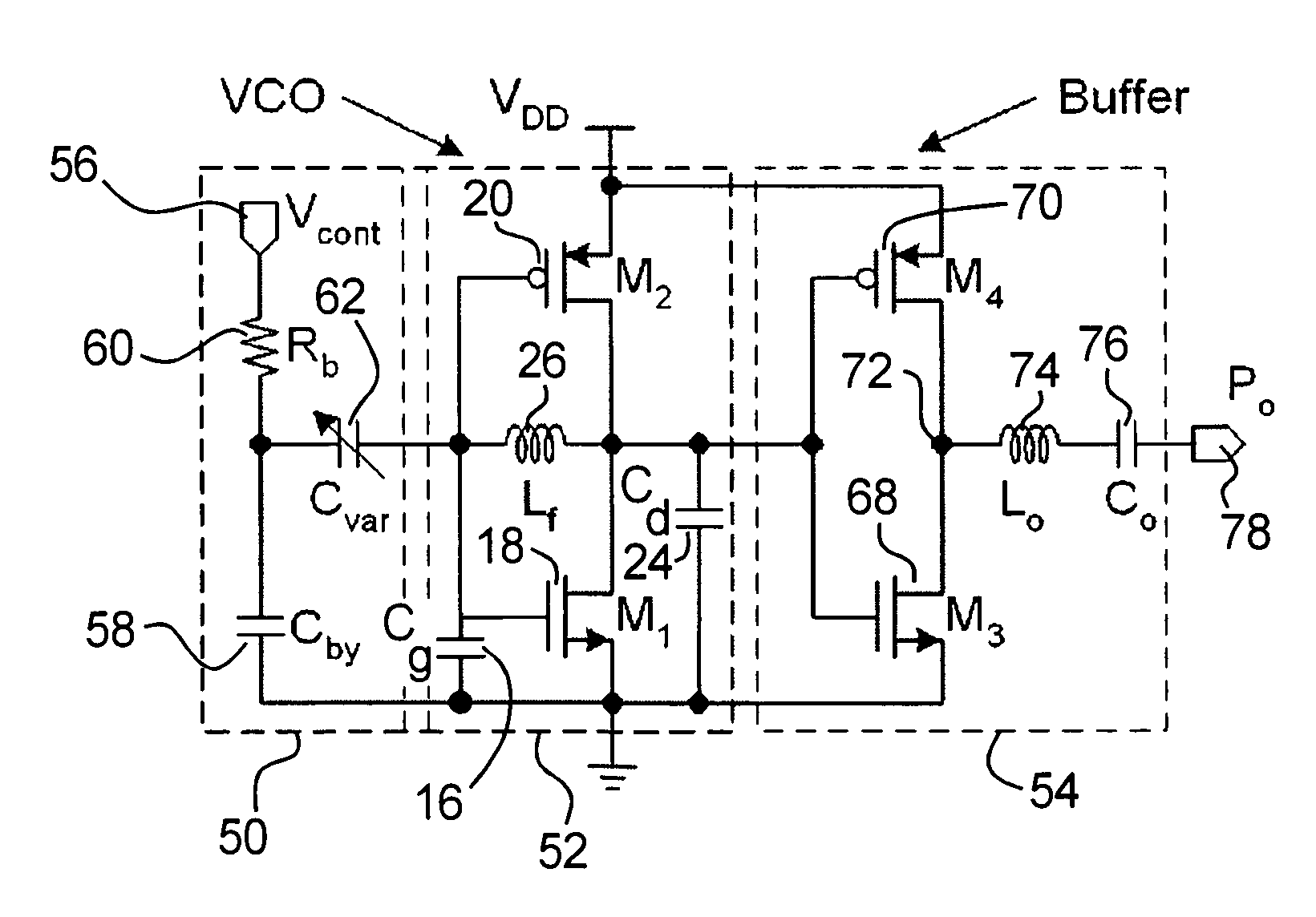
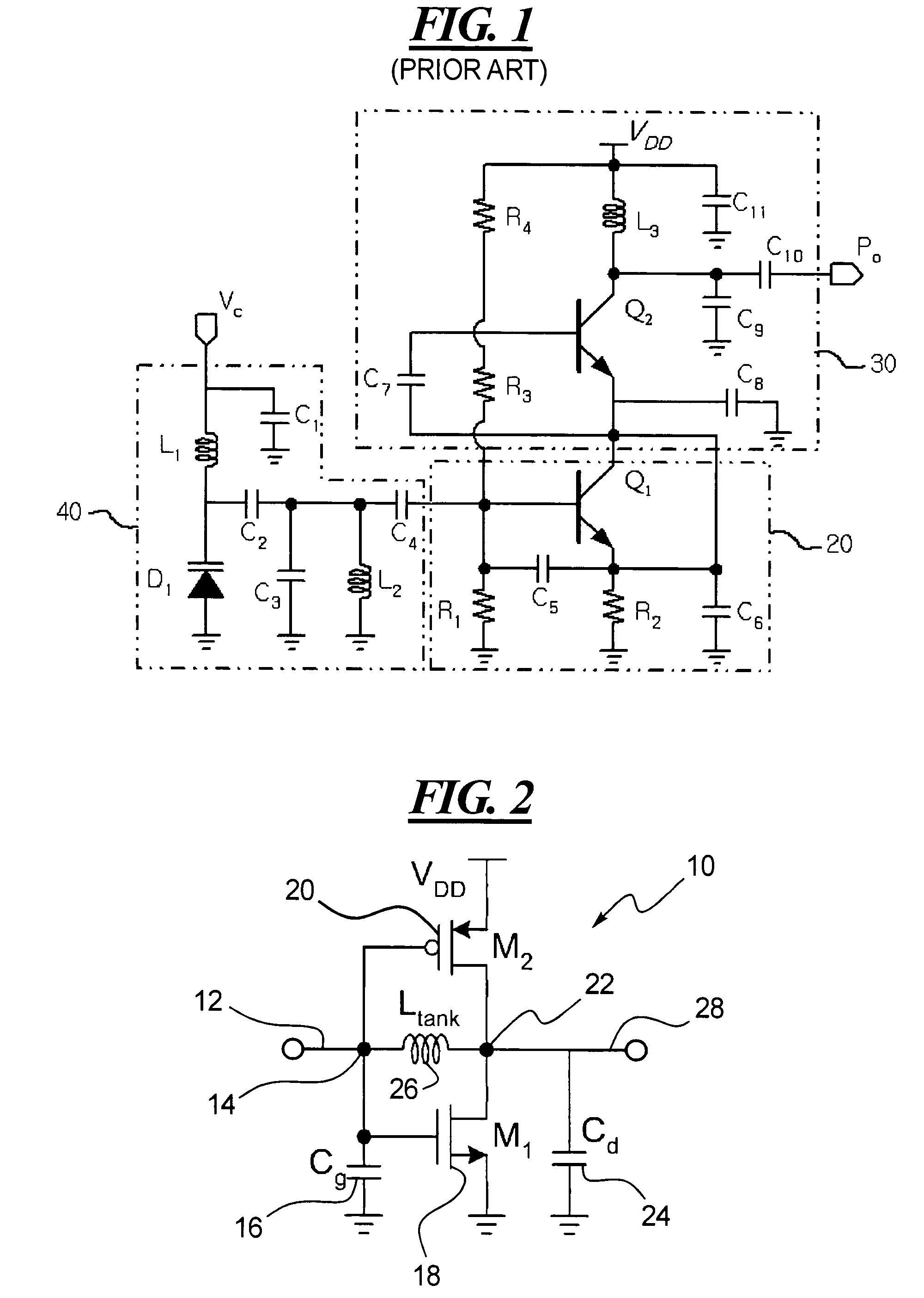
[0024]FIG. 2 shows the present complementary voltage controlled oscillator amplifier core 10. The present oscillator amplifier core 10 may be referred to as a Complementary Colpitts (or C-Colpitts) oscillator. The oscillator core 10 has an input 12 at which a frequency signal is provided to a node 14. The node 14 is connected by a capacitance Cg 16, which is the overall gate-source capacitance, to ground. The node 14 is connected to the gates of first and second transistors 18 and 20, also marked M1 and M2 in FIG. 2. The first transistor 18 is an N-type FET (Field Effect Transistor) that has its source connected to ground. The second transistor 20 is a P-type FET that has its source connected to a supply voltage VDD. The presence of two types of transistors, the N-type and the P-type, is referred to as complementary transistors.

[0025]The drains of the two transistors 18 and 20 are connected together. Thus, the transistors 18 and 20 share a common bias current, since the current flow...


PUM


Abstract

A voltage controlled oscillator is provided. The oscillator has an oscillator amplifier core formed of a complementary pair of FETs connected with their gates in common and connected to share a bias current. An inductance is connected between the common gates and the common drains of the FETs. The inductance may be an inductor element or an inductance of a physical structure of the circuit, such as a bond wire. The voltage controlled oscillator includes a variable capacitor stage connected at the input of the oscillator amplifier stage and a buffer amplifier stage connected at the output of the oscillator amplifier stage. The buffer amplifier of one embodiment includes a pair of complementary FETs having common gates connected to the common drains of the FETs of the oscillator amplifier stage. The buffer amplifier stage also include an inductor and a capacitor connected between common drains of the buffer amplifier FETs and the output.

Description

BACKGROUND OF THE INVENTION[0001]1. Field of the Invention[0002]The present invention relates generally to an electrical oscillator circuit and, in particular, to a voltage-controlled oscillator with complementary transistors.[0003]2. Description of the Related Art[0004]Wireless radio communications systems transmit voice and other data between fixed transceivers and mobile radio communications terminals, or between two mobile terminals, via the propagation of radio frequency (RF) electromagnetic waves. It is essential to the functionality of such wireless communication systems that a stable and accurate generation of oscillating electrical signals be provided. The oscillating signals are supplied by oscillators, such as voltage controlled oscillators, connected in the communications system circuitry. Low phase noise oscillators are important components in wireless communication systems, particularly since phase noise critically affects the sensitivity of wireless transceivers. With...

Claims


Application Information

Patent Timeline
Patent Type & Authority Patents(United States)
IPC IPC(8): H03B5/04
CPCH03B5/1228H03B5/1218H03B5/1243
Inventor KANG, DONG KYUNCHA, CHOONG-YULLEE, SANG-GUG
Owner NEOREACH INC
Why Eureka
Try Eureka