Laser irradiation apparatus, laser irradiation method, and method for manufacturing semiconductor device

a laser irradiation and semiconductor technology, applied in the direction of manufacturing tools, solid-state devices, transistors, etc., can solve the problems of difficult crystal formation, difficult to form crystal grains, so as to improve the annealing efficiency of semiconductor films, enhance the laser annealing efficiency, and prolong the effect of long beams

Inactive Publication Date: 2006-10-24
SEMICON ENERGY LAB CO LTD
View PDF22 Cites 35 Cited by
  • Summary
  • Abstract
  • Description
  • Claims
  • Application Information

AI Technical Summary

Benefits of technology

[0039](a) Although the fundamental wave having a wavelength of about 1 μm is hardly absorbed in a normal thin semiconductor film, when there is an aid of the pulsed laser beam having a wavelength not longer than that of visible light irradiated simultaneously with the fundamental wave, the fundamental wave is absorbed sufficiently in the thin semiconductor film melted by the pulsed laser beam. Therefore, annealing efficiency to the semiconductor film is more enhanced. In the present invention, the wavelength of the fundamental wave is not limited to 1 μm approximately, and any other wavelengths are applicable as long as the wavelengths are absorbed in the melted semiconductor film. This makes it possible to assist the energy of the pulsed laser beam with the energy of the fundamental wave.
[0040](b) When the fundamental wave having a wavelength of about 1 μm is irradiated simultaneously with the pulsed laser beam having a wavelength not longer than that of visible light to the semiconductor film, the fundamental wave is absorbed in the region melted by the pulsed laser beam in the semiconductor film, and the melting state can be kept even after the pulsed laser beam disappears once. On this occasion, it is preferable to increase the output of the fundamental wave appropriately in synchronization with the attenuation of the energy of the pulsed laser beam since the energy given to the semiconductor film can be made constant at a rate per unit time. When such a laser beam is scanned relative to the semiconductor film, it is possible to form the long crystal grain region because the melted region can be moved in the semiconductor film. Furthermore, since the energy given to the semiconductor film is constant at a rate per unit time, the semiconductor characteristic in the long crystal grain region can be made uniform. This is advantageous in enhancing the laser annealing efficiency and in relaxing the design rule because the long beam can be made much lo

Problems solved by technology

It is quartz that is suitable for a material of a substrate applicable for this crystallization, but a quartz substrate is expensive and is very difficult to be processed into a large substrate.
In such a case, it was not possible to form the crystal grains as specifying their positions and sizes.
Although the crystallinity of the semiconductor film in a channel forming region has a serious influence on characteristics of t

Method used


Image

  • Laser irradiation apparatus, laser irradiation method, and method for manufacturing semiconductor device
  • Laser irradiation apparatus, laser irradiation method, and method for manufacturing semiconductor device
  • Laser irradiation apparatus, laser irradiation method, and method for manufacturing semiconductor device

Examples


embodiment mode 1

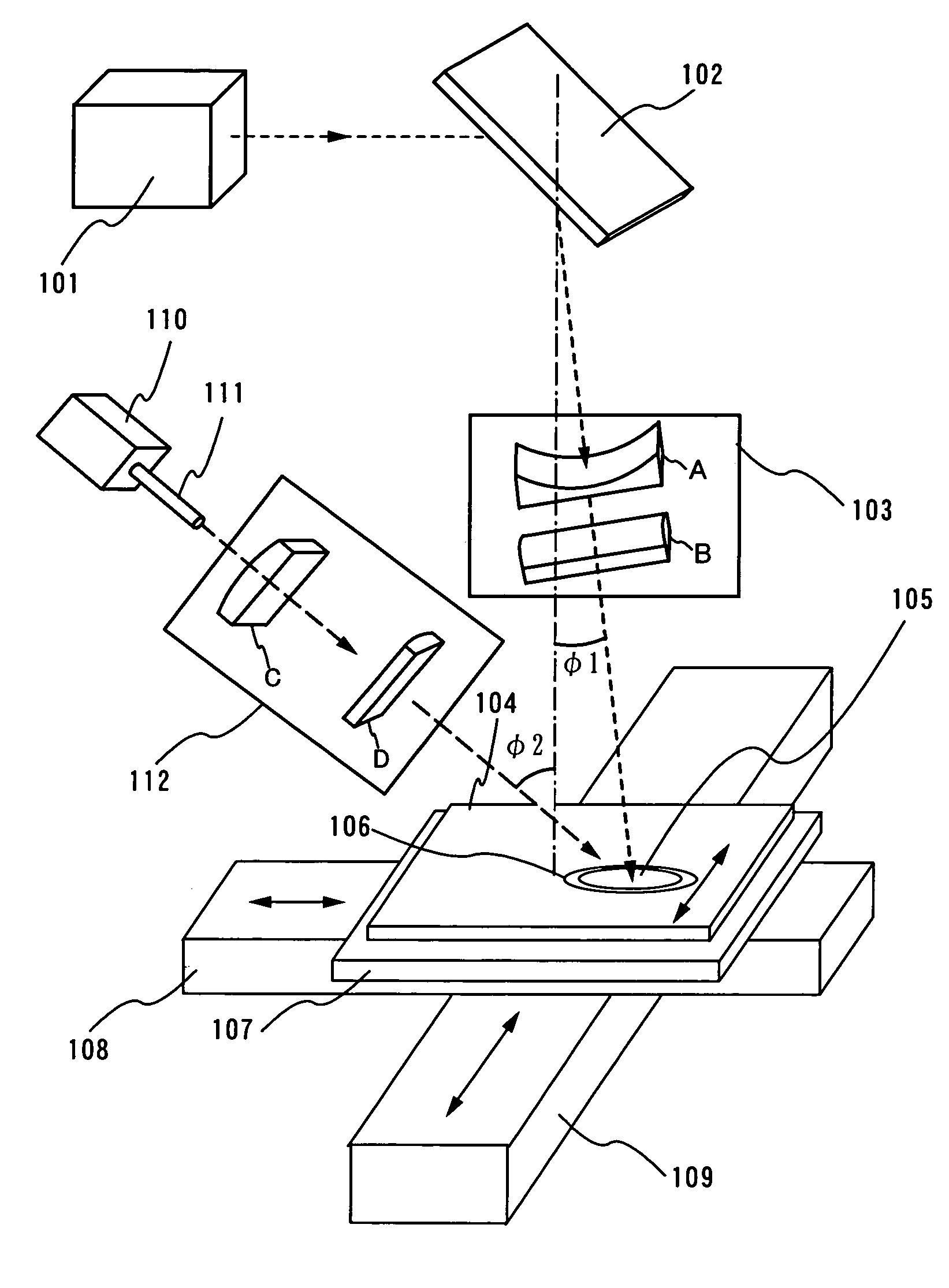
[0062]An embodiment mode of the present invention is explained with FIG. 1. This embodiment mode explains an example in which a long beam 105 and a long beam 106 are formed to irradiate a surface of a semiconductor film 104.

[0063]First, a pulsed laser oscillator 101 with an output of 10 W (Nd: YLF laser, second harmonic) is prepared. The laser oscillator generates in TEM00 mode, and includes a non-linear optical element to convert a laser beam into the second harmonic. The harmonic is not particularly limited to the second harmonic, but the second harmonic is superior to the other higher harmonics in terms of conversion efficiency. The frequency is 1 kHz, and the pulse width is 60 ns approximately. Although a compact solid laser is used in this embodiment mode, a large-scale laser with an output as much as 300 W such as a XeCl excimer laser may be also used.

[0064]Since the laser beam is usually emitted to the horizontal direction, a traveling direction of the laser beam 1 is changed...

embodiment mode 2

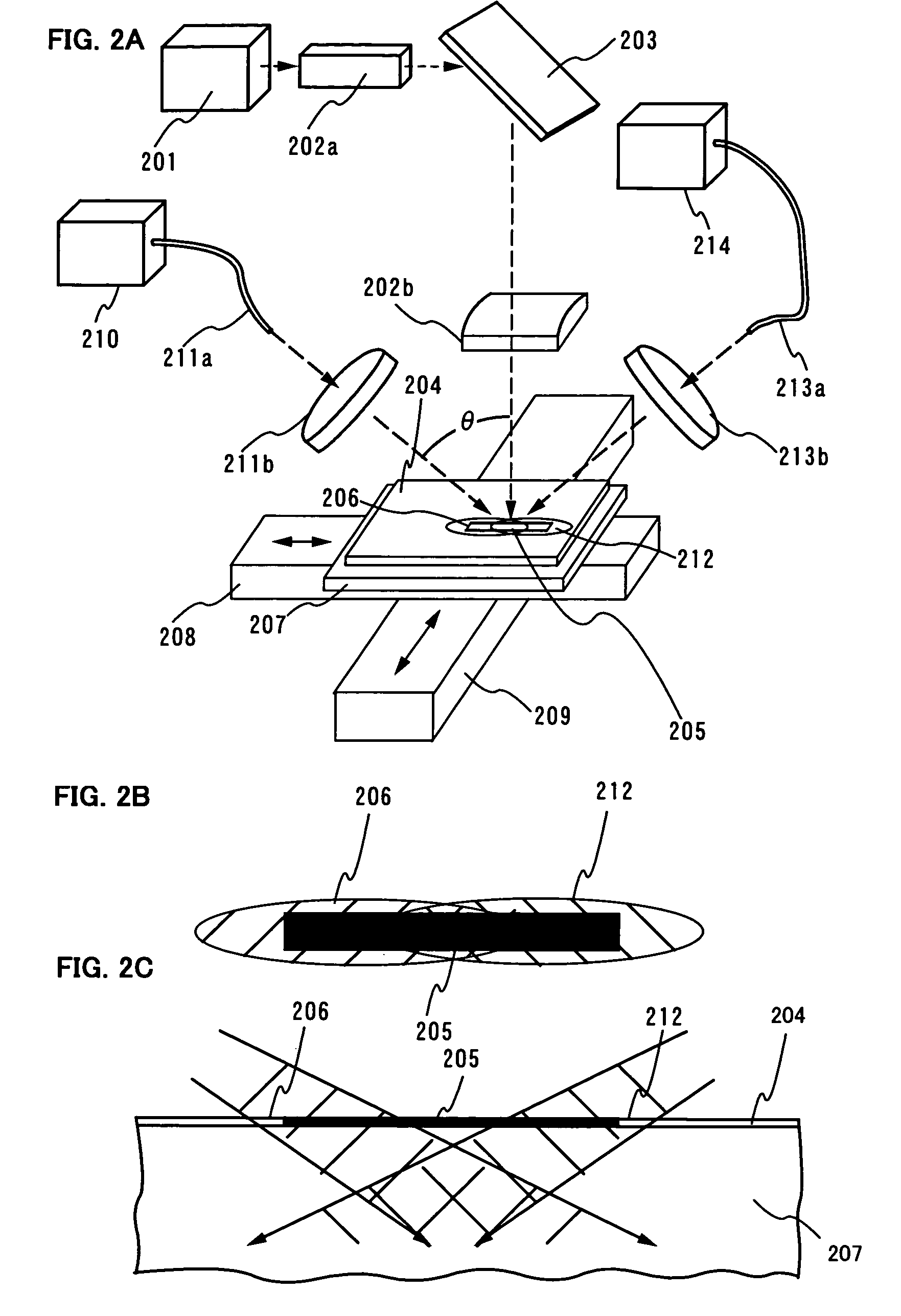
[0070]This embodiment mode explains with FIGS. 2A and 2B an example in which the long beam obtained by shaping the second harmonic shown in the embodiment mode 1 is made much longer by using a plurality of laser oscillators outputting fundamental waves.

[0071]First, a pulsed laser oscillator 201 with an output of 30 W (KrF excimer laser, wavelength of 248 nm) is prepared. The pulsed laser oscillator has a frequency of 100 Hz, and can output 300 mJ per a pulse. The beam spot is processed to have a size of 2 mm×1 mm through an appropriate optical systems 202a and 202b. The beam is reflected by a mirror 203 between the optical systems 202a and 202b. The energy distribution is made uniform, and a homogenizer with a cylindrical lens array and a cylindrical lens combined for example, is used as the optical system. Alternatively, a light pipe or other integrated lens may be used in order to homogenize the energy distribution. When the semiconductor film is crystallized with an excimer laser...

embodiment mode 3

[0077]This embodiment mode explains an example with FIGS. 4A and 4B in which several long laser beams obtained by shaping the second harmonic are combined to form a much longer beam, and furthermore the fundamental wave is used to aid the energy.

[0078]First, four pulsed laser oscillators with an output of 6 W respectively (Nd: YLF laser, second harmonic) are prepared (not shown in the figure). Each of the laser oscillators generates in TEM00 mode and includes a non-linear optical element to convert the laser beam into the second harmonic. The harmonic is not limited to the second harmonic, but the second harmonic is superior to the other higher harmonics in terms of conversion efficiency. The frequency is 1 kHz, and the pulse width is 60 ns approximately. Although a compact solid laser is used in this embodiment mode, a large-scale laser with an output as much as 300 W such as a XeCl excimer laser may be also employed.

[0079]Several reflecting mirrors are used in order to change trav...


PUM

PropertyMeasurementUnit
Thicknessaaaaaaaaaa
Widthaaaaaaaaaa
Wavelengthaaaaaaaaaa

Abstract

An aggregation of crystals extending long in the scanning direction (a long crystal grain region) is formed when a continuous wave laser oscillator (a CW laser oscillator) is employed for annealing the semiconductor film in the manufacturing process of a semiconductor device. The long crystal grain region has a characteristic similar to that of single crystal in the scanning direction, but there is restriction for high integration because of the small output of the CW laser oscillator. pa In order to solve the problem, a pulsed laser beam 1 having a wavelength absorbed sufficiently in the semiconductor film is used in combination with a laser beam 2 having a high output and having a wavelength absorbed sufficiently in the melted semiconductor film. After irradiating the laser beam 1 to melt the semiconductor widely, the laser beam 2 is irradiated to the melted region. And then the laser beam 2 and the semiconductor film are moved relatively while keeping the melting state so as to form the long crystal grain region. The laser beam 2 keeps to be irradiated to the semiconductor film until the laser beam 1 is irradiated, and the output of the laser beam 2 is attenuated when the laser beam 1 is irradiated so as not to give the energy more than is needed so that the very uniform laser annealing becomes possible. Thus the long crystal grain region having a width 10 times as broad as the conventional one can be formed.

Description

BACKGROUND OF THE INVENTION[0001]1. Field of the Invention[0002]The present invention relates to a laser irradiation method and a laser irradiation apparatus to perform the laser irradiation (the laser irradiation apparatus includes a laser oscillator and an optical system to guide a laser beam emitted from the laser oscillator to an object to be irradiated.). In addition, the present invention relates to a method for manufacturing a semiconductor device using the laser irradiation method and the laser irradiation apparatus to perform the laser irradiation. It is noted that the semiconductor device described in this specification includes a general device that can be operated by utilizing the semiconductor characteristic. And thereby a computer, an electro-optical device and the like having the semiconductor device as its component are also included in the semiconductor device.[0003]2. Description of the Related Art[0004]In recent years, research has been extensively conducted on th...

Claims


Application Information

Patent Timeline
IPC IPC(8): H01L21/84H01L21/20H01L21/268H01L21/336H01L21/77H01L27/12H01L29/786
CPCB23K26/0604B23K26/0608H01L27/12H01L27/1285H01L21/268H01L29/78633H01L29/78675
Inventor TANAKA, KOICHIRO
Owner SEMICON ENERGY LAB CO LTD
Why Eureka
Try Eureka