Method for manufacturing light-emitting device

a technology of light-emitting devices and manufacturing methods, which is applied in the manufacture of electrode systems, electric discharge tubes/lamps, discharge tubes luminescnet screens, etc., can solve the problems of deterioration of the el layer, short life of light-emitting elements, and easy oxidation or absorption of moisture, so as to prevent oxygen or moisture, enhance reliability, and prevent the effect of deterioration of light-emitting elements

Inactive Publication Date: 2006-10-31
SEMICON ENERGY LAB CO LTD
View PDF7 Cites 23 Cited by
  • Summary
  • Abstract
  • Description
  • Claims
  • Application Information

AI Technical Summary

Benefits of technology

[0019]It is an object of the present invention to prevent oxygen or moisture from reaching a pixel portion of a light-emitting device without being exposed to heat or UV light, prevent deterioration of the light-emitting element, and enhance the reliability. It is another object of the present invention to seal the light-emitting element with few steps without sealing a drying agent in.

Problems solved by technology

An EL material to form an EL layer deteriorates extremely easily, and is easily oxidized or absorbs moisture due to oxygen or moisture.
Thus, a light-emitting element has a problem of a decline in luminance or short lifetime.
A two-component sealing material is mixed with air bubbles in mixing, a time before bonding after mixing is limited, working efficiency is poor, and thus the two-component sealing material is not used so often.
Although the thermosetting material is cured by heating, a whole element is exposed to high heat for curing, and thus characteristics of the element is deteriorated.
It is difficult to enhance productivity, since the time for curing is long.
In such a bottom emission structure, there is a problem that aperture ratio of a pixel is limited by a structure of a TFT circuit.
It is, however, difficult to arrange a drying agent over a pixel portion, or use an encapsulating can formed of materials that can shield a display light, since the drying agent or the encapsulating can disturbs the display in the top emission structure.
Further, since the drying agent is highly hygroscopic, the drying agent requires careful handling and quick operation in sealing.
There is, however, a fear that air bubbles spreading to the pixel portion will remain in corners when a seal pattern shape for the second sealing material is formed into a square shape, an inverted “c” shape, or a “U” shape, and the two substrates are bonded by dripping the first sealing material having low viscosity thereon.
Although the UV curing sealing method is suitable for sealing an element as described above, the seal pattern has a limitation, when there is a portion (such as a wiring portion of a TFT substrate or a sealing can) through which UV light cannot pass.
Particularly, in the element in which a sealing substrate having a color filter is bonded to the top emission element, it is impossible to fill and seal the space over the pixel portion with UV curing sealing material, since neither a TFT substrate nor the sealing substrate having a color filter can transmit UV light.
In the top emission element in which the transparent electrode exists in a lower portion of the sealing material, the UV light reaches the EL layer, and thus the element is damaged.

Method used


Image

  • Method for manufacturing light-emitting device
  • Method for manufacturing light-emitting device
  • Method for manufacturing light-emitting device

Examples


embodiment mode 1

[Embodiment Mode 1]

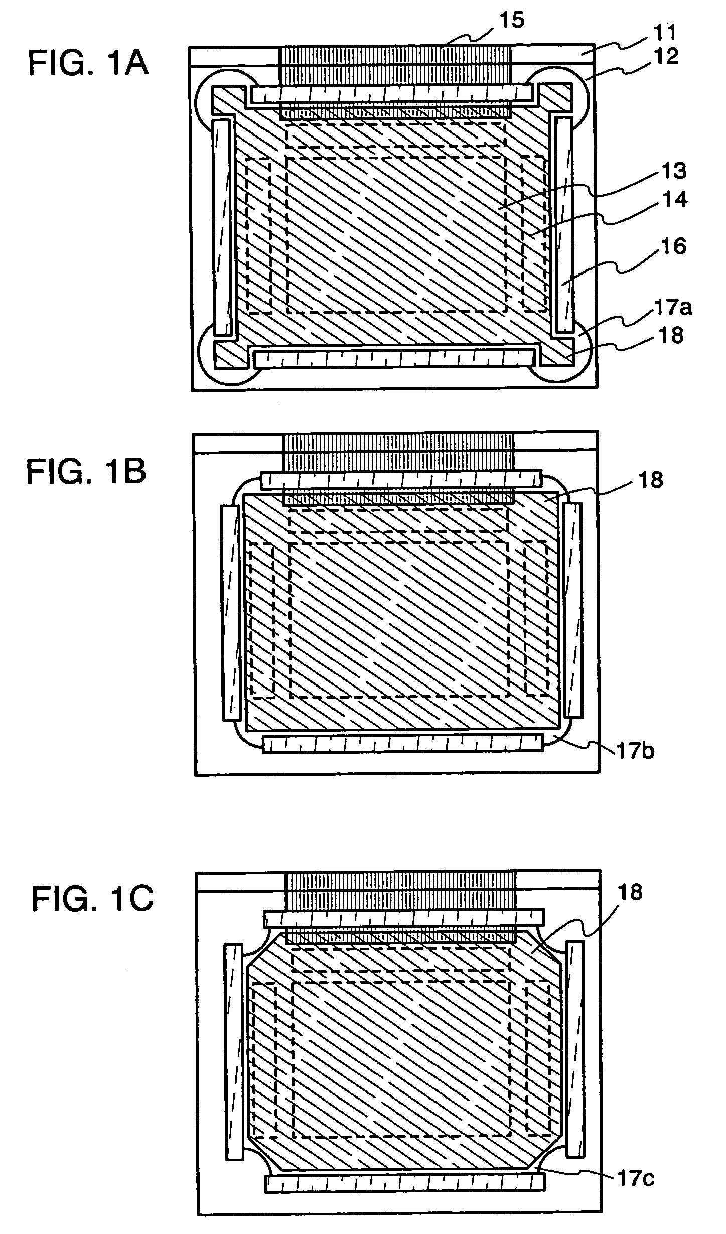
[0075]FIG. 1A is a top view of an active matrix light-emitting device according to the present invention.

[0076]In FIG. 1A, reference numeral 11 denotes a first substrate, reference numeral 12 denotes a second substrate, reference numeral 13 denotes a pixel portion, reference numeral 14 denotes a driver circuit portion, reference numeral 15 denotes a terminal portion, reference numeral 16 denotes second sealing materials, reference numeral 17a denotes a first sealing material, and reference numeral 18 denotes a catalyst for curing the first sealing material.

[0077]There are no specific limitations placed on the material used for the first substrate 11. It is preferable, however, to use substrates having identical thermal expansion coefficients for the first substrate 11 and the second substrate 12 because the two substrates are bonded together. A substrate having light transparency, for example, a glass substrate, a quartz substrate, or a plastic substrate, is used ...

embodiment mode 2

[Embodiment Mode 2]

[0091]A portion of a cross sectional structure of a pixel portion of the present invention is shown here in FIGS. 3A to 3C.

(First Substrate)

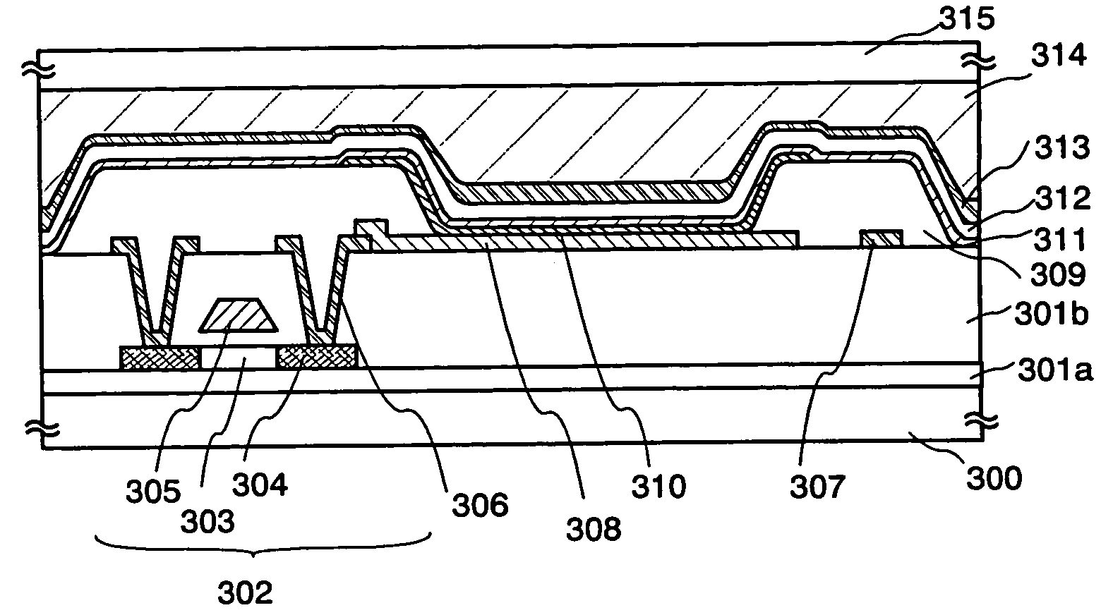
[0092]In FIG. 3A, reference numeral 300 denotes a first substrate, reference numerals 301a and 301b denote insulating layers, reference numeral 302 denotes a TFT, reference numeral 308 denotes a first electrode, and reference numeral 309 denotes an insulator. Reference numeral 310 denotes an EL layer, reference numeral 311 denotes a second electrode, reference numeral 312 denotes a transparent protective layer, reference numeral 313 a catalyst layer, reference numeral 314 denotes a first sealing material, and reference numeral 315 denotes a second substrate.

(TFT Structure)

[0093]The TFT 302 (p-channel TFT) formed on the first substrate 300 is an element for controlling current flowing in the light-emitting EL layer 310, and reference numeral 304 denotes a drain region (or a source region) thereof. Further, reference numeral 306...

embodiment mode 3

[Embodiment Mode 3]

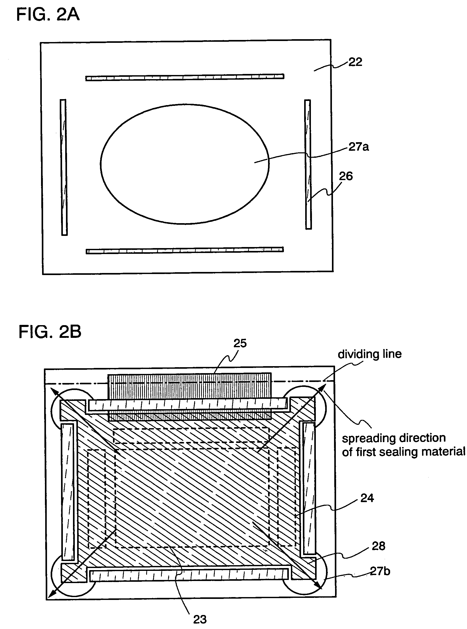
[0114]A case of forming a plurality of pixel portions on one substrate, that is, an example of multiple patterns, is shown in FIGS. 4A to 4E. An example of forming four panels using one substrate is described hereinafter.

[0115]Second sealing materials 32 are formed in a predetermined location on a second substrate 31 by a dispenser in an inert gas atmosphere (FIG. 4A). A material that contains a filler (diameter 6 μm to 24 μm) and has a viscosity of 370 Pa·s is used as a material for the semi-transparent second sealing materials 32. The second sealing material 32 can be formed by a printing method because it has a simple sealing pattern.

[0116]Next, a transparent first sealing material 33 is dripped on the region surrounded by the second sealing materials 32 (with openings in four corners) (FIG. 4B). A highly heat resistant UV epoxy resin added with a photo-oxidation generating material (product name: 2500 Clear, manufactured by Electrolite Cooperation) having an i...


PUM


Abstract

A sealing structure is provided without irradiating a pixel portion of a light emitting element by heat or UV light. By the sealing structure, the reliability is enhanced by blocking out oxygen and moisture, and preventing the deterioration of the light emitting element. The sealing structure in which a whole surface of the pixel portion is covered with a sealing material and which has an excellent sealing property is manufactured without being exposed to heat or UV light. In this case, a catalyst for curing a sealing material is formed as a film on a substrate, and a sealing material for covering a pixel portion is applied to the other substrate. Then, the both substrates are bonded together.

Description

BACKGROUND OF THE INVENTION[0001]1. Field of the Invention[0002]The present invention relates to a method for manufacturing a semiconductor device including a circuit made by using thin film transistors (hereinafter, TFT). For example, the present invention relates to a method for manufacturing a light-emitting device comprising a light-emitting element, which emits fluorescence or phosphorescence upon application of an electric field thereto. The light-emitting element includes a pair of electrodes and a layer containing organic compound (hereinafter, an organic compound layer) that is sandwiched between the pair of electrodes. In this specification, the term light-emitting device includes an image display device, a device for emitting light, or a light source (including a lighting system). Also, the following modules are included in the light-emitting device: a module obtained by attaching a connector such as an FPC (flexible printed circuit), a TAB (tape automated bonding) tape, ...

Claims


Application Information

Patent Timeline
Patent Type & Authority Patents(United States)
IPC IPC(8): H05B33/04H05B33/10H01L51/50H01L51/52
CPCH01L51/5237H01L27/3244H10K59/12H10K50/828H10K50/8426H10K50/844
Inventor NAKAMURA, YASUO
Owner SEMICON ENERGY LAB CO LTD
Why Eureka
Try Eureka