Exposure device and image forming device

a technology of image forming device and exposure device, which is applied in the direction of instruments, optical elements, recording devices, etc., can solve the problems of high material cost, difficult to reduce cost, and difficult to produce lsus of smaller size and adaptability, and achieve the effect of small and inexpensiv

Inactive Publication Date: 2006-10-31
SHARP KK
View PDF11 Cites 13 Cited by
  • Summary
  • Abstract
  • Description
  • Claims
  • Application Information

AI Technical Summary

Benefits of technology

[0019]Various embodiments of the present invention have been made to overcome the above problems. and address the cost and technological problems of LEDs as mentioned above by making the most use of organic EL to apply it to an exposure device, thereby producing an exposure device that is small and inexpensive.

Problems solved by technology

Accordingly, it is difficult to produce LSUs of smaller size and to adapt them to be operated at still higher speeds.
An LED array is generally constructed of a substrate of a III-V group compound semiconductor such as GaAs, resulting in high cost of material.
Further, it requires a technique of precisely arranging a plurality of LED chips each having a plurality of light emissive elements, and also requires a drive circuit chip on a single-crystal silicon substrate to be connected to LED chips of GaAs using wire bonding, making it more difficult to reduce the cost.
Since higher resolution requires emissive elements to be integrated more densely, wire bonding constraining interconnection with the driver IC from being made more densely is particularly problematic.
Further, time division driving requires image data to be rearranged, thereby increasing the scale of circuitry.
Consequently, LED arrays, while smaller than LSUs and thus significantly more advantageous in size, are disadvantageous compared to LSUs in terms of cost and performance and thus have not gained popularity.
An exposure device employing such inorganic ELs, however, requires an alternating-current high voltage pulse with 250 volts for driving the device and has a low response rate at several hundreds of μsec. and other problems, which have hampered its commercialization.
Also, when an organic EL of the surface emission type for use with displays is to be applied in an exposure head of a printer, one serious problem arises as to how to provide the required amount of light for illuminating a photosensitive material.
Further, the organic EL of the surface emission type is characterized by a large angle of radiation, which is advantageous for a display due to a larger angle of field, but causes a problem for an exposure head of a printer because, in an exposure head that requires image optics, a larger angle of radiation results in less efficient use of light in the optics.
Providing this amount of light using an inorganic EL is extremely difficult without compromising the lifetime of the organic EL.
Another problem occurs in conjunction with imaging optics.
In the case of magnifying or reducing optics, the load on imaging optics is increased for removing aberration due to a larger angle of view, so that providing a smaller size is difficult.
On the other hand, in the case of an organic EL of the surface emission type, increasing the emitting area to compensate for an insufficient amount of light as mentioned above results in a correspondingly increased size of the source (i.e. its emitting area).
Consequently, it is theoretically impossible to provide an emitting surface that is larger than the size of the required image spot for optics with a lateral magnification of one time.

Method used


Image

  • Exposure device and image forming device
  • Exposure device and image forming device
  • Exposure device and image forming device

Examples


first embodiment

[0040](First Embodiment)

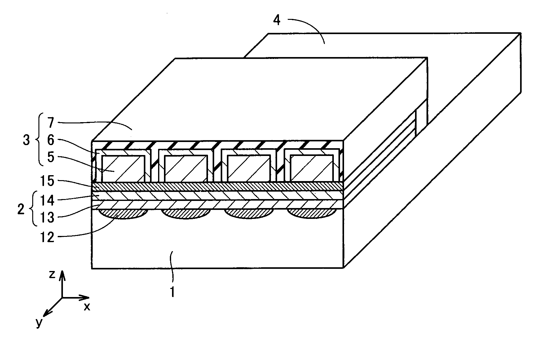
[0041]FIG. 1 shows a schematic cross sectional view of the structure of one exemplary exposure device with an anode provided on a single-crystal silicon substrate 1. The substrate is shown being made of single-crystal silicon as one example. Referring to FIG. 1, the exposure device is provided with a driver circuit portion 4 including drive circuitry, an anode 12, a hole transporting layer 13, an electron transporting and emitting layer 14, a cathode 15, an optical waveguide core layer 5, an optical waveguide clad layer 6, and a shading wall 7. Of the xyz coordinates in FIG. 1, the direction z is the direction of deposition of the layers and the direction y is the direction of edge emission, and an edge emitting structure is employed where an organic EL emissive element 2 emits light in the edge direction (direction y) perpendicular to the direction of deposition of the electrode layers and organic compound layers (direction z).

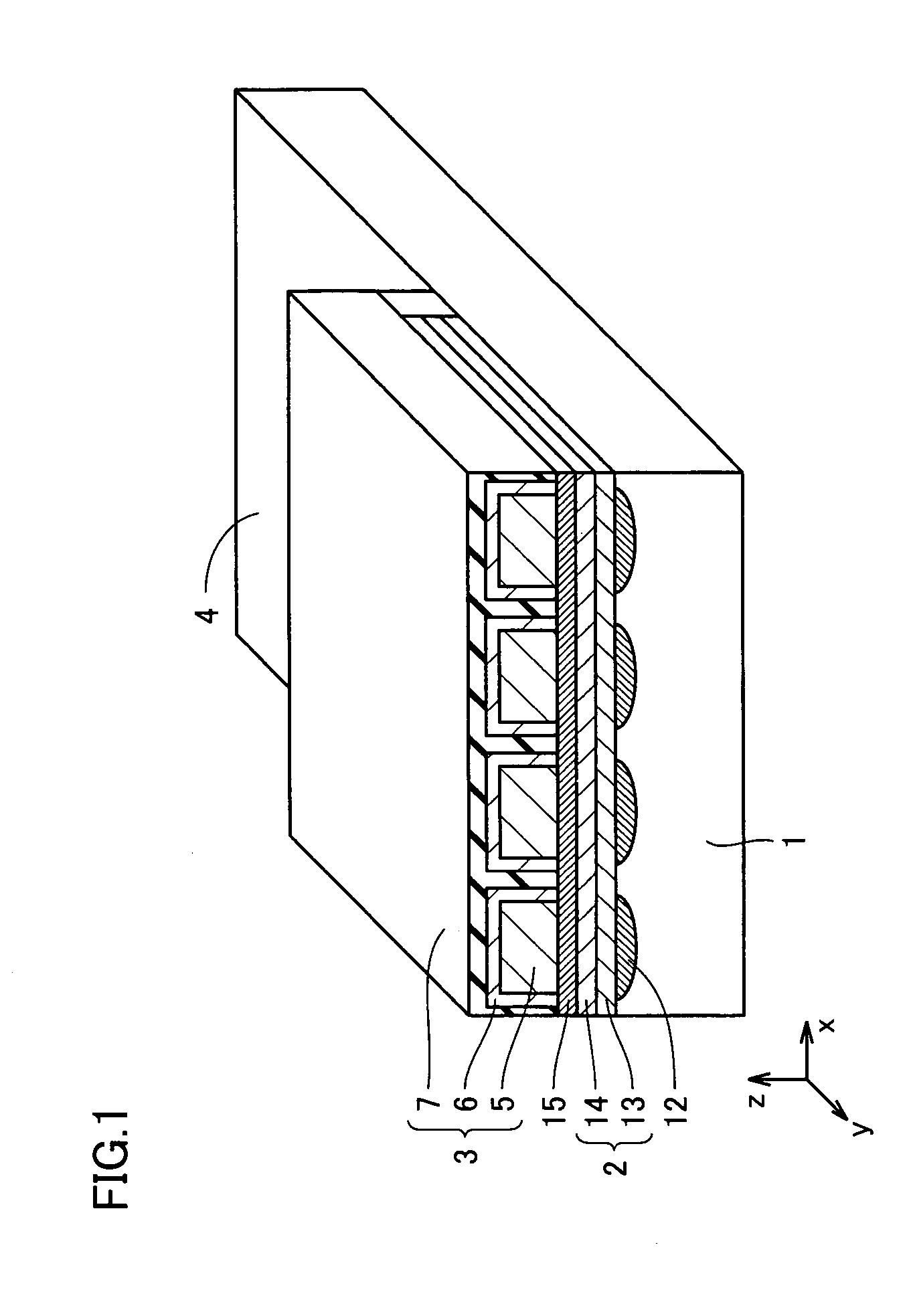
[0042]FIG. 2 shows a schematic ...

second embodiment

[0090](Second Embodiment)

[0091]Turning to FIG. 3, an exposure device according to a second embodiment will be described. The prerequisites for a structure as shown in FIGS. 1 and 2 are that the amount of light propagated along optical waveguide layer 3 is sufficiently larger than the amount of light propagated along organic EL emissive element 2 and that the crosstalk of light in organic EL emissive element 2 is negligible. However, constraints due to the material, such as refractive index, or those due to the structure, such as film thickness, may cause the amount of light propagated along organic EL emissive element 2 to be relatively large. Then, crosstalk of light in organic EL emissive element 2 becomes a problem. Specifically, light emitted from an element adjacent to a non-emissive element is propagated to the non-emissive region so that light is emitted from an edge of the non-emissive region. Crosstalk in the exposure head forms an image in a location that should be a non-i...

third embodiment

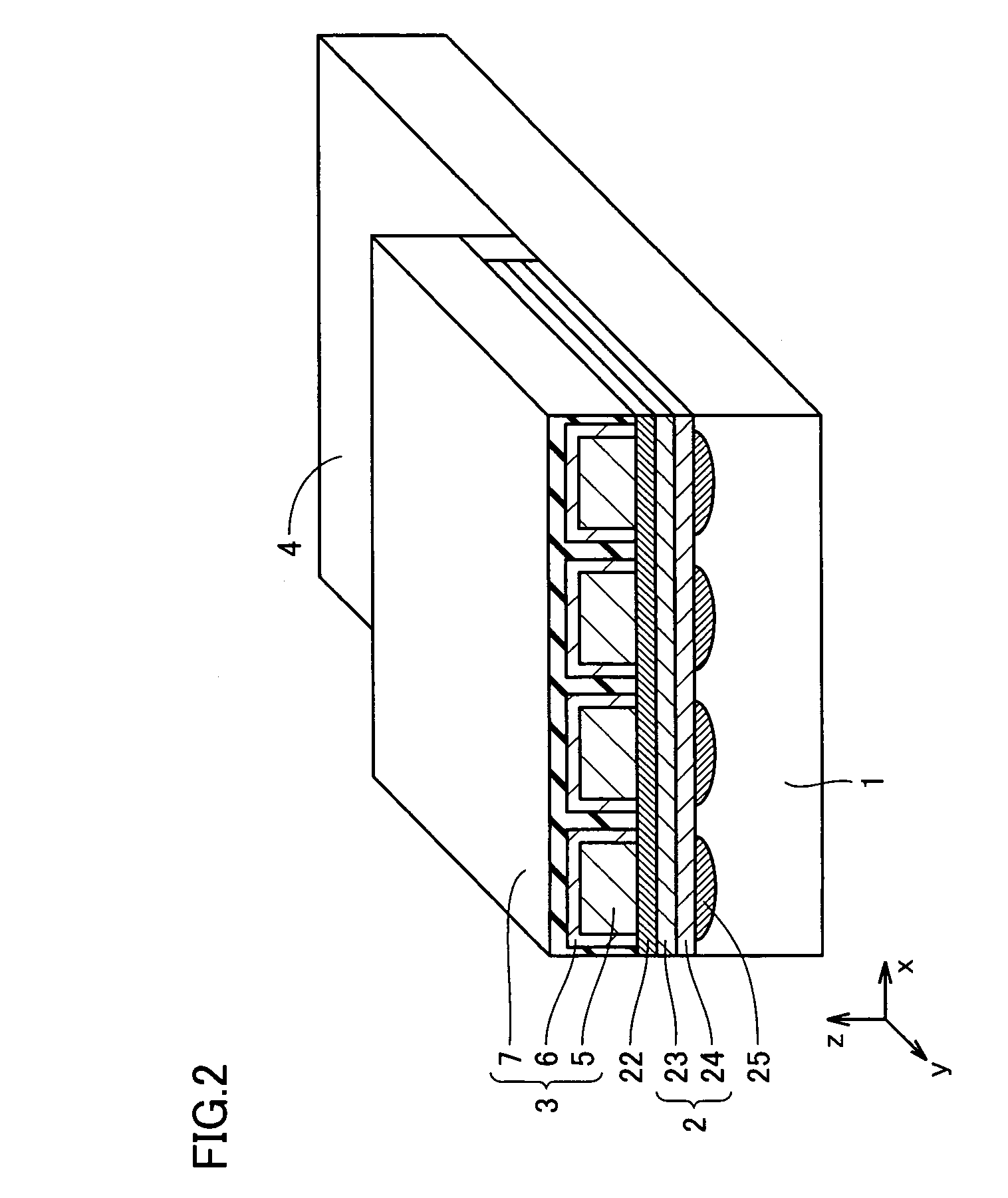
[0093](Third Embodiment)

[0094]Turning to FIG. 4, an exposure device according to a third embodiment will be described. Constructing an exposure device as shown in FIG. 4 can improve the efficiency in light propagation in organic EL emissive element 2 without optical waveguide layer 3.

[0095]The organic compound layers have a three-layer structure with an emitting layer with a refractive index of n4 and sandwiching layers with a refractive index of n5 for sandwiching the emitting layer and having an electron transporting material and a hole transporting material mixed together, where the refractive index of the emitting layer, n4, and the refractive index of the sandwiching layers, n5, satisfy the relationship of n4>n5, and a shading wall that is non-transmissive to light and light-absorbing is provided between adjacent ones of the organic EL emissive elements.

[0096]For example, when organic EL emissive element 2 has a three-layer structure as shown in FIG. 4, organic EL emissive elem...


PUM


Abstract

An emissive element array of a plurality of organic EL elements is arranged linearly on a single-crystal silicon substrate or polycrystalline silicon substrate with a drive circuit including an element switching its respective emissive element. The organic EL emissive elements have an edge emitting structure utilizing light emitted in an edge direction perpendicular to the direction of deposition of electrode layers and organic compound layers, and is constructed such that the emitting area of one emisive element, S, as viewed in the direction of deposition, and the period of emissive elements disposed side by side, d, have the relationship of S>d2. In this way, organic EL techniques can be applied to provide the required amount of light exposure and to produce an exposure device that is small and inexpensive.

Description

TECHNICAL FIELD[0001]The present invention relates to exposure devices and image forming devices used with digital electrophotographic devices for exposing a photosensitive material to light to form a visible image with toner, and more particularly, to optical printer heads employing organic electroluminescent (EL) elements.BACKGROUND ART[0002]Conventionally, LSUs for scanning with a laser beam or an LED array with LEDs disposed in one line are commonly used as exposure devices for creating an electrostatic latent image in a photosensitive material. An LSU requires a polygon mirror rotated at tens of thousands of revolutions per minute (rpm), has a long optical path and requires a large number of optical components such as a lens. Accordingly, it is difficult to produce LSUs of smaller size and to adapt them to be operated at still higher speeds.[0003]An LED array is generally constructed of a substrate of a III-V group compound semiconductor such as GaAs, resulting in high cost of ...

Claims


Application Information

Patent Timeline
Patent Type & Authority Patents(United States)
IPC IPC(8): B41J2/447H01L27/32H01L51/50H05B33/02B41J2/44B41J2/45B41J2/455G02B6/122H04N1/036H05B33/00
CPCB41J2/45
Inventor IWAMATSU, TADASHINISHIO, SHIGERUINUI, TETSUYA
Owner SHARP KK
Why Eureka
Try Eureka