
Sample selection and data alignment circuit

a data alignment and sample selection technology, applied in the field of high-speed data communication, can solve the problems of not teaching the realignment of the over-sampled data signal, the delay element and resistor are known to be highly dependent, and the signals transmitted from one integrated circuit to another cannot be reliably sampled on a predetermined clock signal

Inactive Publication Date: 2006-11-14
IBM CORP
View PDF5 Cites 18 Cited by
  • Summary
  • Abstract
  • Description
  • Claims
  • Application Information

AI Technical Summary

Benefits of technology

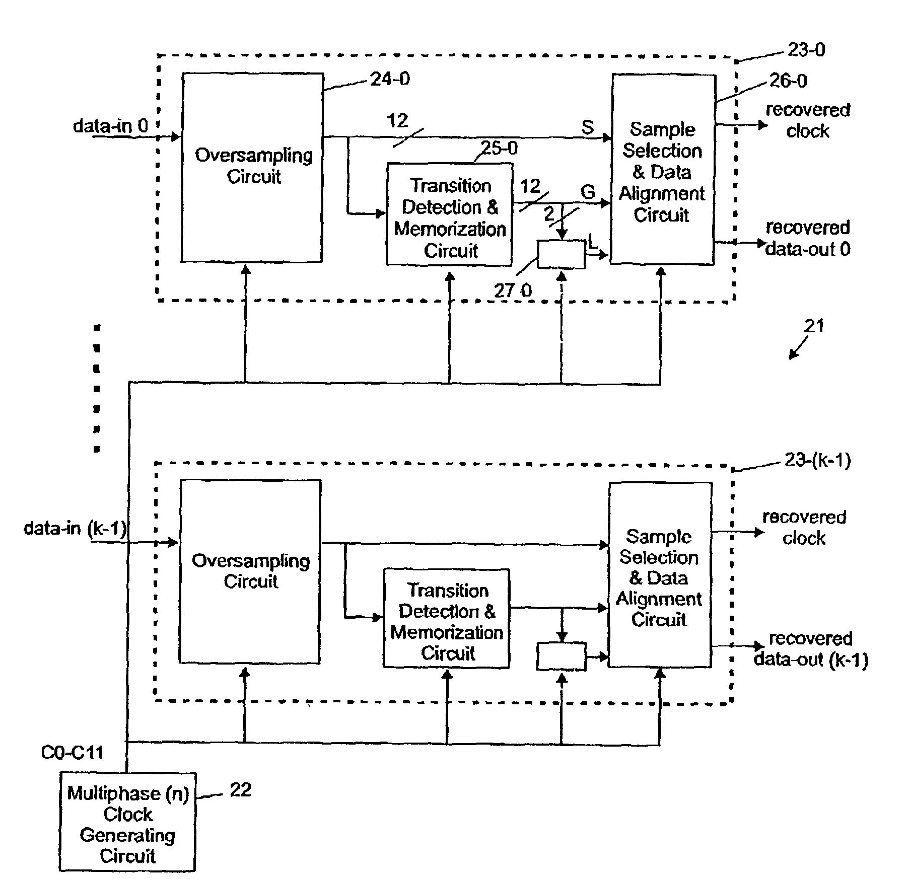
[0008]It is another object of the present invention to provide a sample selection and data alignment that consumes minimal surface area when implemented in a silicon chip and can be designed according to the LSSD rules for high testability.
[0010]The SSDA of the present invention is able to recover (retime) a selected data on a predefined clock phase signal without introducing additional data perturbations. The SSDA circuit works synchronously with the multiple phase clock signal and its performance does not depend on the manufacturing process because it does not require any resistor or delay line as in standard similar circuits.

Problems solved by technology

In high speed data communications between integrated circuits (systems), it often occurs that the signals transmitted from one integrated circuit to another one cannot be reliably sampled on a predetermined clock signal.
Unfortunately, over sampled data signals come out as multiple signals, each one being related to a particular phase of the multiple phase clock signal.
For instance, U.S. Pat. No. 6,026,134 covers some data recovery issues using an over sampling technique but does not teach how the over sampled data signal may be realigned on a predefined phase of the multiphase clock signal.
However, delay elements and resistors are known to be highly dependent on manufacturing process variations.
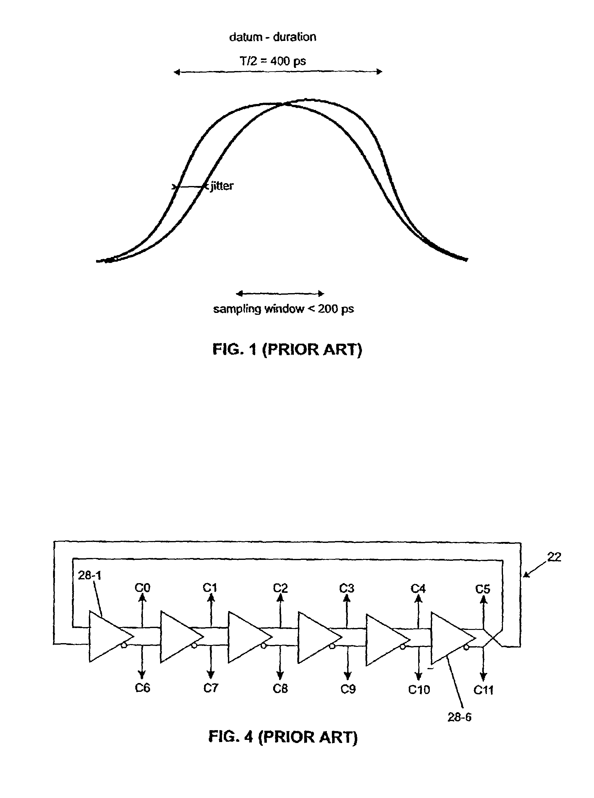
In addition, there is a significant signal jitter induced by power supply variations.
As a consequence, these circuits are therefore inadequate for high speed serial binary data communication applications.
Moreover, the section that selects the best sampled signal for each bit of the incoming data implies a combinatory logic to demultiplex the selected sampled signal which may cause additional delay or data skew problems in such high speed applications due to the existence of different paths.
Finally, these circuits are relatively complex, consuming thereby much silicon area and are not adequate for LSSD (Level Sensitive Scan Design) which allows excellent testability.

Method used


Image

  • Sample selection and data alignment circuit
  • Sample selection and data alignment circuit
  • Sample selection and data alignment circuit

Examples


Embodiment Construction

[0024]In conventional DR and CDR circuits, two different phases of a reference clock signal delayed in time are used, one to detect a transition and the other to capture the data for subsequent processing. However, it should be recognized that because of possible metastability problems, the particular sampled signal (or sample) obtained by performing the sampling at a data transition (logic state 1 to 0 or vice-versa) is not reliable to accurately locate the exact position of the transition and the detection is even more complicated by the presence of glitches and false detections. As a result, the conventional techniques of sampling that have been practiced so far appear to be close to limit as the clock frequencies continue to sharply increase.

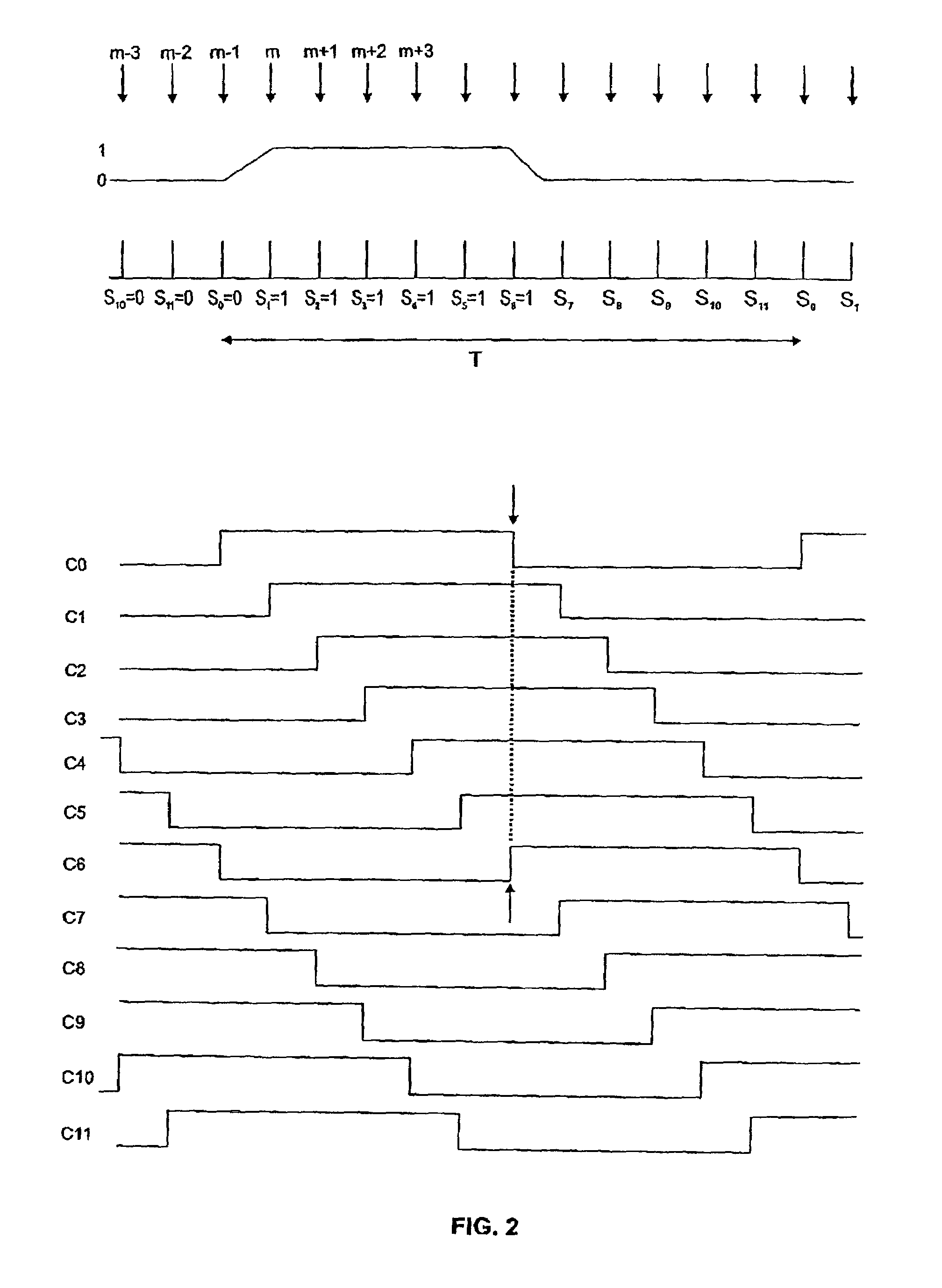
[0025]FIG. 2 is an example of a typical data bit stream, assuming that the clock frequency is the half of the incoming data frequency (the frequency of the multiphase clock is usually the same or half of the frequency of the incoming data si...


PUM


Abstract

There is disclosed a sample selection and data alignment circuit that is able to recover (retime) a data on a predefined phase of a multiphase clock signal. A plurality of over sampled signals (G0, . . . , Gn−1) is obtained by over sampling an incoming serial binary data (bits) stream with the n phases (G0, . . . , Gn−1) of a multiphase clock signal. A reliable over sampled signal is selected according to a selected signal (G0, . . . , Gn−1) generated by an edge detector which designates which over sampled signal is the best for subsequent processing.

Description

CROSS REFERENCE TO RELATED APPLICATIONS[0001]Cross reference is hereby made to U.S. patent applications Ser. No. 10 / 280,285, entitled “Method and circuit for recovering a data signal from a stream of binary data” and Ser. No. 10 / 280,286, entitled “Transition detection, validation and memorization circuit” which were filed on even date herewith.FIELD OF THE INVENTION[0002]The present invention relates to high speed data communications and more particularly to a sample selection and data alignment circuit for selecting the sampled signal in a set of over sampled signals as being the best to represent the recovered data and then aligning it with a predefined phase of a locally generated multiphase clock signal.BACKGROUND OF THE INVENTION[0003]In high speed data communications between integrated circuits (systems), it often occurs that the signals transmitted from one integrated circuit to another one cannot be reliably sampled on a predetermined clock signal. In this case, it is common...

Claims


Application Information

Patent Timeline
IPC IPC(8): H04L7/00H04L7/033H04L25/06
CPCH04L7/0338H04L25/068H04L25/069
Inventor VALLET, VINCENTHAUVILLER, PHILIPPE
Owner IBM CORP
Learn More