Plasma enhanced atomic layer deposition (PEALD) equipment and method of forming a conducting thin film using the same thereof

a technology of atomic layer deposition and forming equipment, which is applied in the direction of chemical vapor deposition coating, coating, electric discharge tubes, etc., can solve the problems of increasing the deposition time required for obtaining a thin film of the desired thickness, unable to achieve excellent step coverage, and insufficient performance of conventional cvd methods for forming thin films in nano-scale thickness on a substrate or achieving excellent step coverage, etc., to achieve high quality

Inactive Publication Date: 2006-11-21
ASM KOREA LTD
View PDF13 Cites 132 Cited by
  • Summary
  • Abstract
  • Description
  • Claims
  • Application Information

AI Technical Summary

Benefits of technology

[0027]The object of the present invention is to construct a reactor within which the process gases are replaced in a short period of time in order to process atomic layer deposition method, and also within which a plasma is generated over the surface area of a substrate, thereby even if a conductive thin layers are deposited, without causing the aforementioned electrical short in the reactor, and at the same time the atomic layer deposition process can easily be carried out, and is to provide an apparatus for forming a high quality thin film by using the plasma enhanced atomic layer deposition method according to the present invention.
[0028]Another object of the present invention is to provide a method of forming efficiently a good quality of thin film, even if the source gases do not react with each other easily or the reactivity is very weak, by using a plasma enhanced atomic layer deposition apparatus according to the present invention.

Problems solved by technology

However, as the density of semiconductor devices recently continues to increase from micrometers to nanometers, conventional CVD methods do not perform satisfactorily in forming a thin film uniformly in thickness in nano scale on a substrate or achieving an excellent step coverage.
In particular, in case of high aspect ratio, in turn large step difference, such as contact holes, vias or trenches, of small dimensions than micrometer (micron), difficulty exists in forming a thin film having uniform composition regardless of high aspect ratios in various patterns such as contacts, via holes or trenches over the entire surface of the substrate.
Accordingly, use of a conventional CVD equipment, in which supply and removal of process gases cannot be made at a fast rate at the speed within several seconds, may increase the deposition time required for obtaining a thin film of a desired thickness because the longer time needed for replacing the process gas.
Increased deposition time reduces the number of wafers to be processed per unit time by one equipment, thereby increasing the processing cost.
As the deposition time increases, the number of wafers that can be processed with each equipment decreases, thereby, the cost of process increases.
However, the gas outlet tube 122 is relocated away from the substrate 110, the volume of the reaction chamber 114 increases, thereby the process cost increases due to the fact that the amount of gas for the same process step increases, and furthermore there is a difficulty of increased process time for supplying and removing gases or replacing process gases for the process of sequentially supplying various types of process gases.
Later such undesirably deposited layer of thin film becomes not only the cause of undesirable micro-particles(contaminants) detrimental to the subsequent processing steps, but also the cause of potentially erratic operation of the parts inside the reaction chamber 114.
Also, the volume of the reaction chamber can not be reduced significantly enough, in order to reduce the processing time for ALD processes.
In the conventional ALD process, in case that the source gases react with each other easily, even a small amount of residual source gases may cause the undesirable generation of particles(contaminants), and therefore, it may be necessary to extend the time of purging.
In the conventional ALD method aforementioned, when the source gases with low reaction rate are used, there is a slow reaction on the substrate, thereby, there may be a problem of lack of deposition of thin film.
However, when this apparatus is used for forming a conductive thin film, a plasma may not be generated because of the fact that two electrodes used for applying RF power for plasma generation are electrically shorted due to the formation of a conductive thin film, and therefore, a conductive thin film may not be formed by using this apparatus along with the plasma enhanced atomic layer deposition method disclosed in the present invention.

Method used


Image

  • Plasma enhanced atomic layer deposition (PEALD) equipment and method of forming a conducting thin film using the same thereof
  • Plasma enhanced atomic layer deposition (PEALD) equipment and method of forming a conducting thin film using the same thereof
  • Plasma enhanced atomic layer deposition (PEALD) equipment and method of forming a conducting thin film using the same thereof

Examples


experimental embodiment 1

[Experimental Embodiment 1]

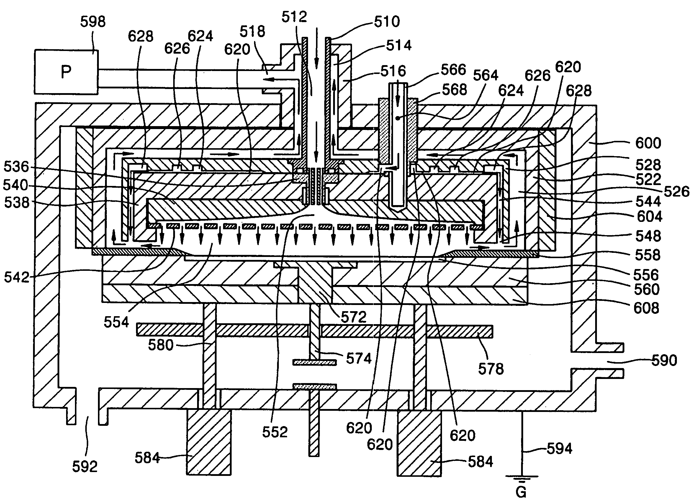
[0082]Following the best mode for carrying out the present invention described above, a thin film using Titanium Nitride(TiN) is formed by the conducting thin film formation method in accordance with the present invention of the plasma enhanced atomic layer deposition method. For this experimental, embodiment, to supply a source gas, 160 sccm of Argon(Ar) gas and Titanium Tetra-Chloride(TiCl4) carried by Argon(Ar) gas of 100 sccm which passes through a source container were supplied through the shower head 540 in a reactor loaded with a substrate. For the process of supplying a purge gas, 100 sccm of Hydrogen(H2) gas, 60 sccm of Nitrogen(N2) gas and Argon gas of 100 sccm were fed through the reactor. Through the orifice of the radio frequency power connection terminal 566, 20 sccm of Argon gas was supplied continuously. The substrate temperature was set at 350° C., the RF power was set at 150 W, and the pressure was set at 3 Torr. The duration of the sourc...

experimental embodiment 2

[Experimental Embodiment 2]

[0083]By using the plasma enhanced atomic layer deposition method according to the present invention, a conductive thin film of Titanium was formed. Similarly to Experimental Embodiment 1 described above, for the source gas supply step, 230 sccm of Argon gas and TiCl4(Titanium Tetra-Chloride) carried by Argon gas of 100 sccm which passes through a source container was supplied to the shower head assembly 540, 542. For the purge gas supply step, 100 sccm of Hydrogen(H2) gas and 230 sccm of Argon gas were supplied. Through the orifice of the radio frequency connection terminal, 20 sccm of Argon gas was supplied. The substrate temperature was set at 380° C., the RF power was set at 200 W and the pressure was set at 3 Torr. The duration of the source gas supply was 0.2 second, the purge gas was supplied for 5.8 seconds. During the purge gas supply time of 5.8 seconds, for the first 2.0 seconds, the RF power was switched off and only the purge gas was supplied....


PUM

PropertyMeasurementUnit
diameteraaaaaaaaaa
lengthaaaaaaaaaa
lengthaaaaaaaaaa

Abstract

A plasma enhanced atomic layer deposition (PEALD) apparatus and a method of forming a conductive thin film using the same are disclosed. According to the present invention of a PEALD apparatus and a method, a process gas inlet tube and a process gas outlet tube are installed symmetrically and concentrically with respect to a substrate, thereby allowing the process gas to flow uniformly, evenly and smoothly over the substrate, thereby forming a thin film uniformly over the substrate. A uniquely designed showerhead assembly provides not only reduces the volume of the reactor space, but also allows the process gases to flow uniformly, evenly and smoothly throughout the reation space area and reduces the volume of the reaction space, and the smaller volume makes it easier and fast to change the process gases for sequential and repeated process operation.

Description

CROSS-REFERENCE TO RELATED APPLICATION DATA[0001]This application claims priority from PCT International Application No. PCT / KR01 / 01333 filed Aug. 6, 2001.BACKGROUND OF THE INVENTION[0002]1. Field of the Invention[0003]The present invention relates to a plasma enhanced atomic layer deposition (PEALD) apparatus and method of forming a thin film using the same. Particularly, the present invention relates to a PEALD apparatus and method of forming a thin film using the same, whereby a thin film is formed to an atomic layer thickness by periodically supplying time-divisional (sequential) combination of process gases to a reactor, during which plasma is generated adequately and synchronously with process gases on top of a substrate in order to accelerate the process reaction and facilitate more efficient reaction.[0004]2. Description of the Related Art[0005]As semiconductor integration technologies advance, process methods for depositing a thin film uniformly and conformally become incre...

Claims


Application Information

Patent Timeline
Patent Type & Authority Patents(United States)
IPC IPC(8): H01L21/44H01L21/311C23C16/455C23C16/44C23C16/509H01J37/32
CPCC23C16/4412C23C16/45508C23C16/45519C23C16/4554C23C16/45544C23C16/45565C23C16/45591C23C16/50C23C16/5096H01J37/32082H01J37/3244H01J37/32449H01L21/28562H01L21/3141H01L21/318H01L21/0228H01L21/0217
Inventor LEE, CHUN SOOOH, MIN SUBPARK, HYUNG SANG
Owner ASM KOREA LTD
Why Eureka
Try Eureka