Production method for silicon single crystal and production device for single crystal ingot, and heat treating method for silicon crystal wafer

a production method and single crystal technology, applied in the field of silicon single crystal production method and production device for single crystal ingot, and heat treatment method of silicon crystal wafer, can solve the problems of reducing the production efficiency affecting the leakage characteristics, and increasing the time per production cycle of single crystal ingot, so as to achieve stable supply and high quality

Inactive Publication Date: 2006-11-28
SUMCO TECHXIV
View PDF24 Cites 21 Cited by
  • Summary
  • Abstract
  • Description
  • Claims
  • Application Information

AI Technical Summary

Benefits of technology

[0027]It is a first object of the present invention to determine further suitable growth conditions to obtain defect free single crystals so that high quality silicon wafers, free from grown-in defects, can be stably supplied.
[0028]It is a second object of the present invention to provide a heat treating method for uniforming oxide precipitates in a silicon wafer in a simple process for silicon prefect crystals.
[0029]It is a third object of the present invention to provide a production device and a method for single crystal ingots to produce silicon perfect crystals wherein the time required for the production process can be decreased and the production efficiency of silicon perfect crystals can be improved.

Problems solved by technology

For an operator to start the disassembly operation, the hot zone must be sufficiently cooled, and for this cooling it normally takes about six hours for a conventional device, which increases the time per production cycle of a single crystal ingot, and drops production efficiency.
These oxide precipitates negatively affect the leak characteristics near the surface layer, but oxide precipitates which exist in the bulk function as a gettering site, which captures heavy metal, Fe and Cu, etc., which has a negative influence on the device yield.
However, this method alone is insufficient for a quality silicon wafer, and the density of oxide precipitates in the bulk and the uniformity of radial distribution are demanded, which is one of the important characteristics of a silicon wafer.
Crystal defects generated during the growth of a CZ silicon single crystal obtained by a Czochralski method (CZ method) negatively affect the reliability of the gate oxide film of an MOS device and on PN junction leak characteristics.
With this method, however, the decrease in defects is limited, and defects become huge.
With this method proposed by Horai et al, however, manufacturing to obtain defect free single crystals is extremely difficult depending on the growth conditions.
Also, when an ingot of a silicon single crystal is produced setting the conditions to the range proposed by Horai et al, the portion of a perfect crystal (defect free crystal) is relatively small, and in terms of a stable supply of silicon wafers without grown-in defects in the industrial process, this method has the problem of uncertainty.
The reason why oxide precipitates are introduced into a perfect crystal wafer by heat treatment is probably because oxide precipitates are generated in the wafer by the growth of oxide precipitate nuclei along with the heat treatment of the wafer, and in a perfect crystal, the wafer radial distribution of oxide precipitation may be very non-uniform in some cases.
However, it is almost impossible to adjust the growth conditions of a perfect crystal to solve such non-uniformity because the growth conditions of a perfect crystal are in an extremely narrow range, and manufacturing a perfect crystal where oxide precipitation distribution is uniform is very difficult.
The above mentioned non-uniform distribution of oxide precipitation is probably because the density distribution of point defects, which strongly relates to the generation of oxide precipitate nuclei, is non-uniform.
This paper, however, does not report on a perfect crystal, and in this case, void defects, due to the coagulation of voids, exist inside the OSF ring, and dislocation clusters, due to the coagulation of interstitial silicon, exist outside the OSF ring, so the method disclosed in this report cannot be directly applied to a perfect crystal.
If the oxygen density is low, on the other hand, the oxide precipitation distribution in the plane cannot be uniform.
And if oxide precipitates are generated even in the device activation layer zone in the surface layer by setting the oxygen density high, this will negatively affect the device yield, and industrial implementation is very difficult.
In the case of low oxygen density where the DZ layer (non-oxide precipitation layer on the surface layer) can exist, on the other hand, oxide precipitation distribution cannot be uniform, so it is difficult to apply the heat treatment method reported by Kissinger et al for industrial implementation.
This method, however, is to make the oxide precipitate density to within about a 1 digit range (uniforming) by the heat treatment of samples with different oxygen densities, and not for solving the non-uniformity of precipitation due to the difference of point defect distribution generated in the crystal growth stage.
Therefore, with this method, it is difficult to achieve a uniformity of oxide precipitation behavior in the diameter direction of crystals or in the plane of the wafer, and it is not possible to stably manufacture wafers having a DZ layer with uniform oxide precipitates.
Another problem of this method is that the complicated thermal process takes time and labor, which considerably aggravates the productivity of products.

Method used


Image

  • Production method for silicon single crystal and production device for single crystal ingot, and heat treating method for silicon crystal wafer
  • Production method for silicon single crystal and production device for single crystal ingot, and heat treating method for silicon crystal wafer
  • Production method for silicon single crystal and production device for single crystal ingot, and heat treating method for silicon crystal wafer

Examples


embodiment a1

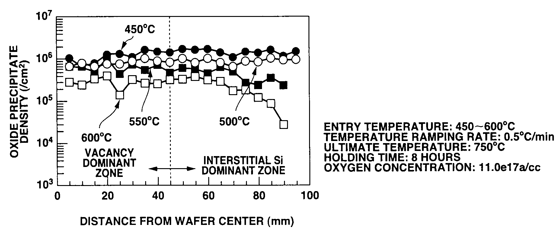
[0128]We studied growth conditions to obtain perfect crystals using various growth conditions. Table A1 shows the result. Experiments were performed using a crystal which diameter is 200 mm. The distribution of crystal defects can be studied by observing the surface of the crystal after soaking the crystal in etchant, but in this embodiment, the distribution of defects was studied by performing non-stirring Secco etching for voids and dislocation clusters, and by performing light etching after oxidizing heat treatment for three hours at 780° C., then for 16 hours at 1000° C. for OSF. The in-crystal temperature gradient in the pulling axis direction at each location in the radius direction was determined by a global heat-transfer analysis in the growth device currently established.

[0129]Table A1 shows the range of the growth speed where a perfect crystal was obtained under each growth condition. Here the conditions where the range of growth speed is not indicated are conditions under...

embodiment a2

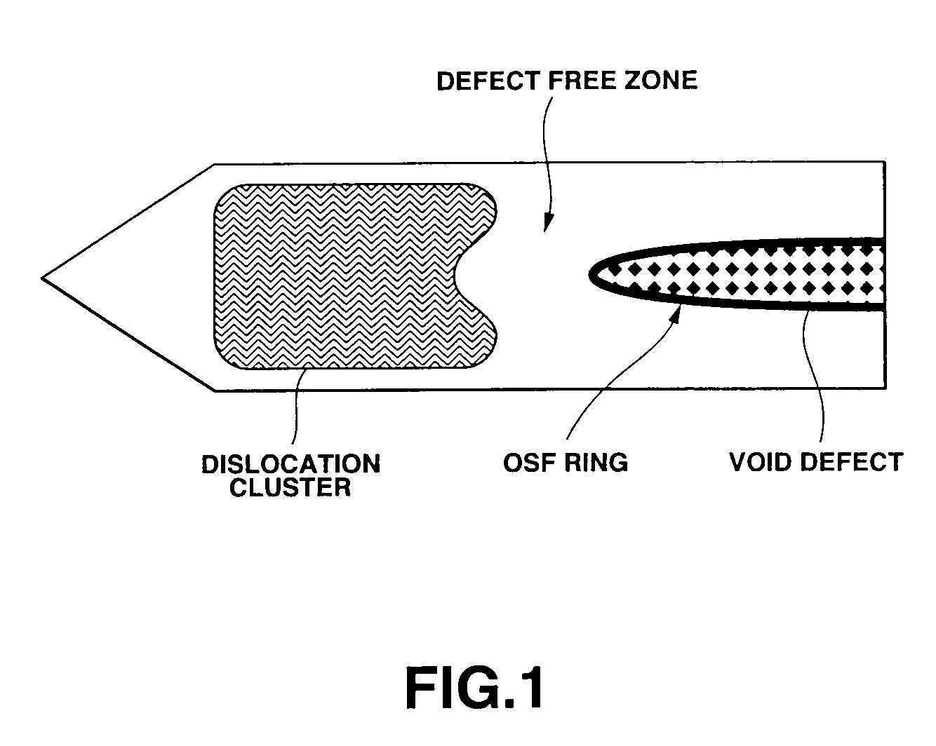
[0133]When a crystal is grown at a constant pulling speed under the growth conditions determined in Table A1, the growth conditions may gradually be deviated from the optimum growth conditions because of the change of the in-crystal temperature gradient during growth. If this state is left alone, a crystal ingot, which is deviated from the defect free growth conditions, as shown in the conceptual diagram in FIG. 1, is produced, so it is necessary to guide the conditions to be optimum by making appropriate changes.

[0134]In the embodiment A2, the pulling speed is changed to guide the conditions to be optimum in such a case. And as Table A2 shows, a perfect crystal was obtained by changing the pulling speed V following up with the change of the length of the crystal.

[0135]

TABLE A2predetermined conditions of pulling speedPresent inventionCrystalExistenceExistencelengthG1 centerPulling speedV / G centerofPulling speedV / G centerof(mm)(° C. / mm)(mm / min)(mm2 / ° C. min)defects(mm / min)(mm2 / ° C. m...

embodiment a3

[0136]This embodiment is for indicating that a perfect crystal can be obtained by changing the distance between the silicon melt and the heat shielding element when the conditions are gradually deviated from the optimum growth conditions because of the change of the in-crystal temperature gradient during growth, in the same way as the embodiment A2 (Table A3).

[0137]

TABLE A3Predetermined conditions on distance betweenSi melt and heat shielding elementPresent inventionDistance betweenDistance betweenCrystalPullingSi melt andExistenceSi melt andExistencelengthspeedheat shieldingG1 centerV / G centerofheat shieldingG1 centerV / G centerof(mm)(mm / min)element (mm)(° C. / mm)(mm2 / ° C. min)defectselement (mm)(° C. / mm)(mm2 / ° C. min)defects00.43702.7860.154Yes702.7860.154Yes1000.43702.720.158Yes702.720.158Yes2000.43702.6430.163Yes702.6430.163Yes3000.43702.5610.168No702.5610.168No4000.43702.5020.172No702.5020.172No5000.43702.4120.178Yes682.4430.176No6000.43702.3580.182Yes662.4860.173No7000.43702.291...


PUM

PropertyMeasurementUnit
temperatureaaaaaaaaaa

Abstract

A method for growing a silicon crystal by a Czochralsky method, wherein, let a pulling speed be V (mm / min) and an average value of an in-crystal temperature gradient in a pulling axis direction within a temperature range, a silicon melting point to 1350° C., be G (° C. / mm), V / G ranges from 0.16 to 0.18 mm2 / ° C. min between a crystal center position and a crystal outer periphery position, and a ratio G outer / G center of an average value G of an in-crystal temperature gradient in a pulling axis direction within a temperature range, a silicon melting point to 1350° C., at a crystal outer surface to that at a crystal center is set to up to 1.10 to thereby obtain a high-quality perfect crystal silicon wafer. Such a perfect crystal silicon wafer, wherein an oxygen concentration is controlled to up to 13×1017 atoms / cm3, an initial heat treatment temperature is at least up to 500° C. and a temperature is raised at up to 1° C. / min at least within 700 to 900° C., thereby making uniform a wafer radial distribution to an arbitrary oxygen precipitation density level.

Description

TECHNICAL FIELD[0001]The present invention relates to a method for producing a silicon single crystal by a Czochralski method, and more particularly to a production method for silicon single crystals to obtain high quality silicon wafers free from grown-in defects.[0002]The present invention also relates to a heat treating method for silicon single crystal wafers, and more particularly to a heat treating method for silicon single crystal wafers concerning perfect crystals fabricated by a Czochralski method.[0003]The present invention also relates to a Czochralski method-based production device for silicon single crystals.BACKGROUND ART[0004][CZ Method-Based Single Crystal Ingot Production Device][0005]A method for pulling a single crystal by a Czochralski method (CZ method) is a known technology, and a CZ method-based single crystal ingot production device is widely used. To obtain a single crystal by a CZ method, a single crystal is pulled out of a melt. Some single crystal ingot p...

Claims


Application Information

Patent Timeline
Patent Type & Authority Patents(United States)
IPC IPC(8): C30B33/02C30B15/00C30B15/14C30B29/06
CPCC30B15/14C30B15/203C30B15/206C30B29/06C30B15/00
Inventor NAKAMURA, KOZOSAISHOJI, TOSHIAKINAKAJIMA, HIROTAKASADOHARA, SHINYANISHIMURA, MASASHIKOTOOKA, TOSHIROUSHIMANUKI, YOSHIYUKI
Owner SUMCO TECHXIV
Why Eureka
Try Eureka