Semiconductor device and method for fabricating the same
a semiconductor and semiconductor technology, applied in the direction of semiconductor devices, electrical equipment, transistors, etc., can solve the problems of disadvantageous leakage current flowing along the dislocation loop defect layer, difficult for the conventional method for fabricating a semiconductor, and inability to provide a desired dopant profile of the transistor, etc., to suppress the increase in leakage current flow and increase the concentration of dopants
- Summary
- Abstract
- Description
- Claims
- Application Information
AI Technical Summary
Benefits of technology
Problems solved by technology
Method used
Image

Examples
first embodiment
[0053]A first embodiment of the present invention will be described below with reference to the accompanying drawings.
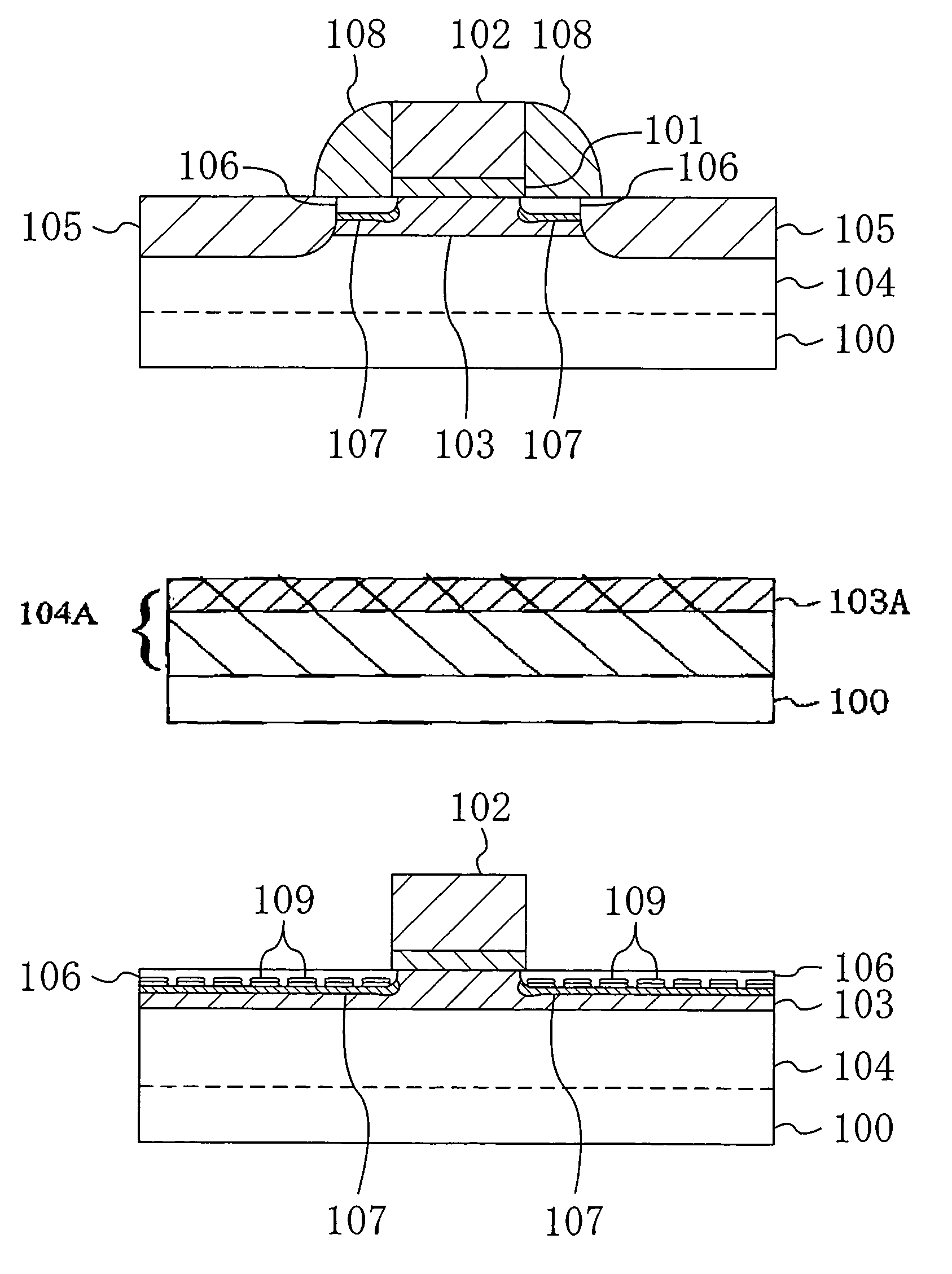
[0054]FIG. 1 shows a cross-sectional construction of a MIS transistor according to the first embodiment of the present invention.
[0055]Referring to FIG. 1, a gate insulating film 101 of silicon oxide is formed on the main surface of a semiconductor substrate 100 of p-type silicon (Si), for example. On the gate insulating film 101, a gate electrode 102 of polysilicon is formed. On the both side surfaces of the gate electrode 102, sidewalls 108 of silicon nitride are formed.
[0056]In a region of the semiconductor substrate 100 located below the gate insulating film 101, a p-diffused channel layer 103 is formed by implanting indium (In) ions which are heavy ions with a relatively large mass number.
[0057]In a region of the semiconductor substrate 100 deeper than the diffused channel layer 103, a germanium (Ge)-containing layer 104 is formed by implanting ions, such as ger...
second embodiment
[0085]A second embodiment of the present invention will be described below with reference to the accompanying drawings.
[0086]FIGS. 6A to 6C, 7A to 7C, and 8A to 8C are sectional views showing process steps of a fabricating method of a MIS transistor according to the second embodiment of the present invention step by step.
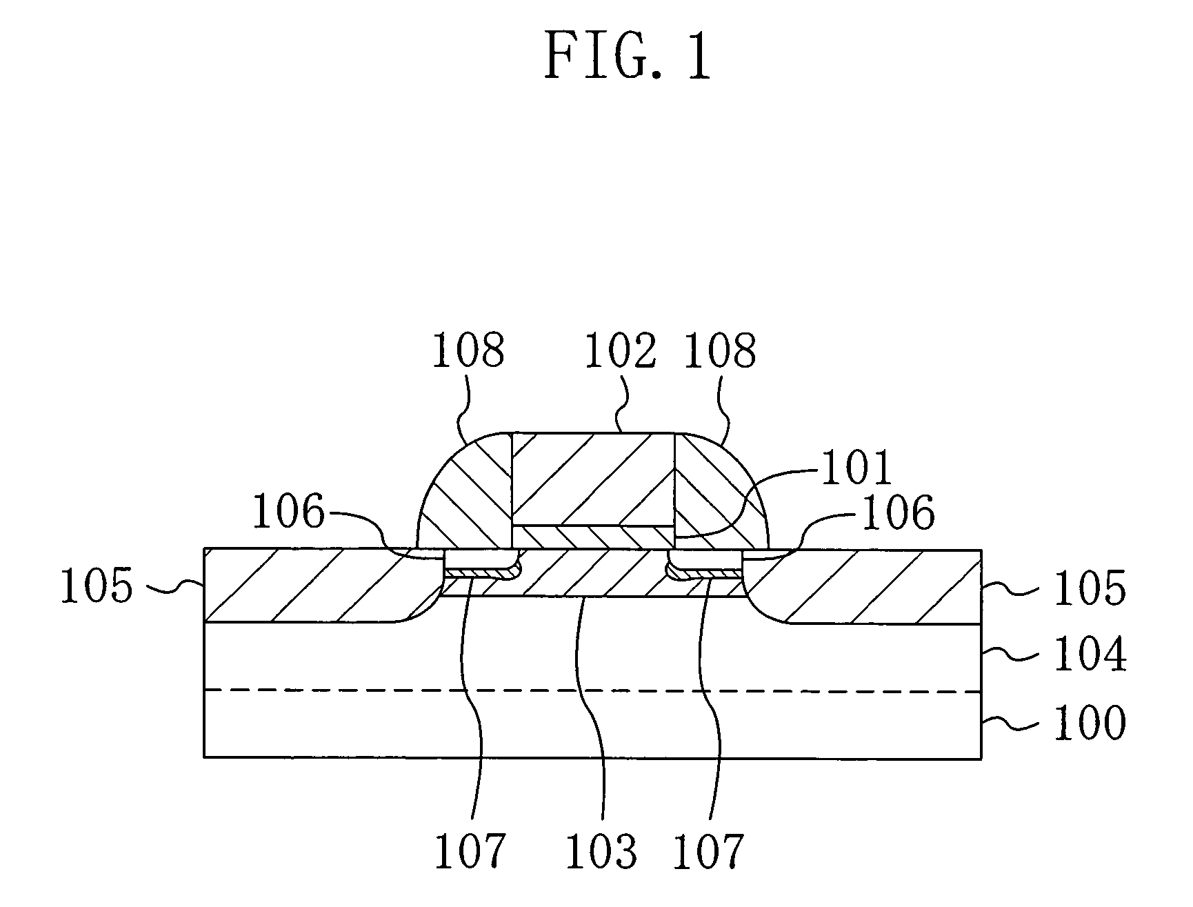
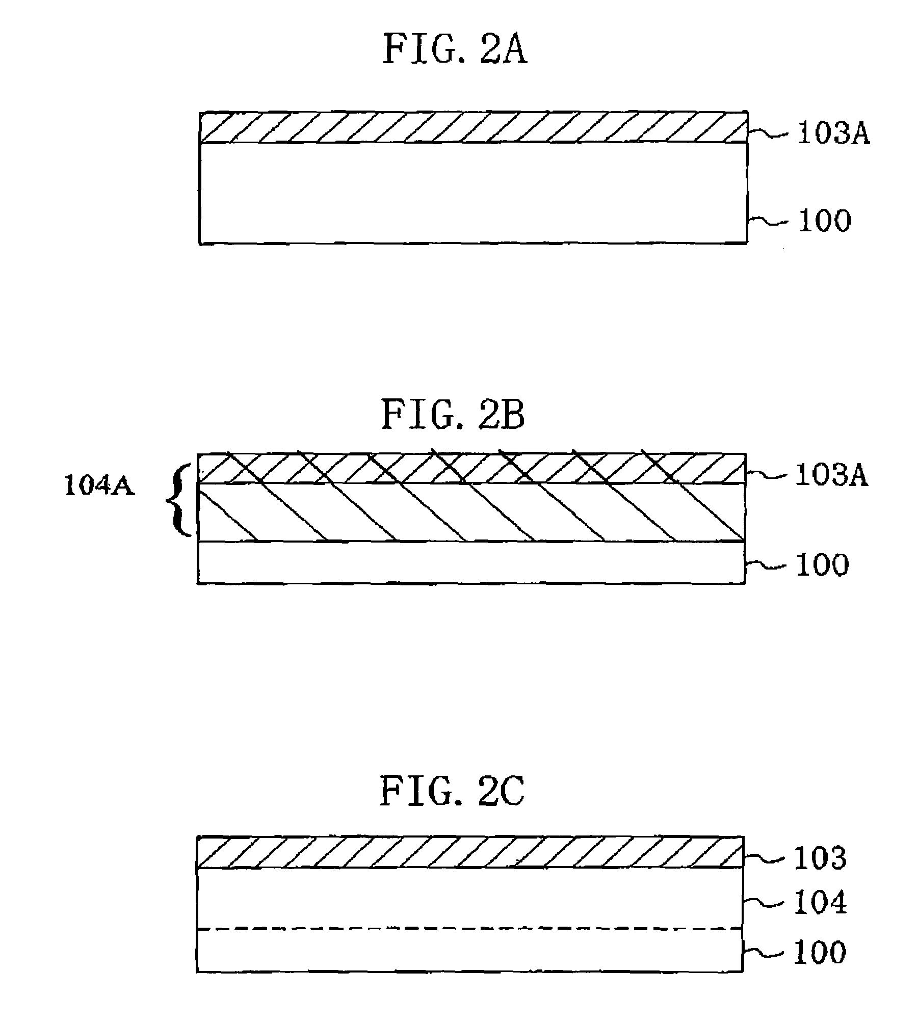
[0087]First, as shown in FIG. 6A, p-type dopant ions with a relatively large mass number, such as indium (In) ions, are implanted into a channel formation region of a semiconductor substrate 100 made of p-type silicon at an implantation energy of about 70 keV and a dose of about 5×10¹³ / cm2. A p-doped channel layer 103A is thus formed.
[0088]Subsequently, as shown in FIG, 6B, germanium (Ge) ions, for example, belonging to group IV elements are implanted into the upper portion of the semiconductor substrate 100 at an implantation energy of about 250keV and a dose of about 1×10¹⁶ / cm2, thereby forming an amorphous layer 104A expanding from the substrate surface to a regi...
third embodiment
[0117]A semiconductor device including a strained silicon layer according to a third embodiment of the present invention will be described below with reference to the accompanying drawings.
[0118]FIG. 11A shows a cross-sectional construction of a MIS transistor according to the third embodiment of the present invention. The description of the components shown in FIGS. 11A to 11C that are the same as those shown in FIG. 1 will be omitted by retaining the same reference numerals, and only the difference between the two figures will be described.
[0119]Referring to FIG. 11A, a buffer layer 110 of silicon germanium (Si1−xGex, where 0100. On the buffer layer 110, a strained silicon layer 111 having a thickness of 20 to 50 nm is formed by epitaxially growing silicon.
[0120]As shown in FIG. 11B, when silicon (Si) is epitaxially grown on the buffer layer 110 having a larger lattice constant than silicon, the lattice constant of the resultant strained silicon layer 111 becomes larger (strained)...
PUM
 Abstract
Description
Claims
Application Information
 - R&D
- Intellectual Property
- Life Sciences
- Materials
- Tech Scout
- Unparalleled Data Quality
- Higher Quality Content
- 60% Fewer Hallucinations
Browse by: Latest US Patents, China's latest patents, Technical Efficacy Thesaurus, Application Domain, Technology Topic, Popular Technical Reports.
© 2025 PatSnap. All rights reserved.Legal|Privacy policy|Modern Slavery Act Transparency Statement|Sitemap|About US| Contact US: help@patsnap.com