Light emitting device

a light-emitting device and light-emitting technology, which is applied in the direction of thermoelectric devices, organic semiconductor devices, solid-state devices, etc., can solve the problems of poor adhesion to the organic surface, inability to oxidize, and poor stability of tft, so as to improve the carrier injection

Inactive Publication Date: 2006-11-28
SEMICON ENERGY LAB CO LTD
View PDF18 Cites 103 Cited by
  • Summary
  • Abstract
  • Description
  • Claims
  • Application Information

AI Technical Summary

Benefits of technology

[0017]It is therefore an object of the present invention to provide the light emitting element that has a mechanism to prevent the light emitting element from quenching due to the removal of the energy produced by recombination of carrier on the light emitting layer, and also improve the carrier injection without using influential materials to TFT characteristics such as alkali metals and alkaline earth metals that are used conventionally.
[0018]In order to resolve the aforementioned problems, the present invention can form donor levels between the respective lowest unoccupied molecular orbitals (LUMOs) between a cathode and an organic compound layer. This is accomplished by doping an organic compound that functions as an electron donor (hereinafter referred to as donor molecules) for applying electrons to the organic compound layer that contacts the cathode. Injection of electrons from the cathode and transmission of the injected electrons can therefore be performed with good efficiency. Further, there are no problems such as excessive energy loss accompanying electron movement and changes in quality of the organic compound layer itself, and therefore an increase in the electron injecting characteristics can be achieved, along with a lowering of driver voltage, regardless of the work function of the cathode material.
[0019]In addition, there is no problem in that the donor molecules diffuse to reduce TFT characteristics, and therefore the characteristics of a light emitting device can be improved without any of the pitfalls present when alkaline metals or alkaline earth metals are used.
[0021]For cases in which an electric charge transfer complex is formed by the donor molecules in the electron transmitting region, if the electric charge transfer complex exists in an interface with the light emitting layer, this structure can prevent problems in which energy generated due to carrier recombination in the light emitting layer is transferred to the non-light emitting electric charge transfer complex, thus optically quenching light.

Problems solved by technology

However, Mg is easily oxidizable, instable, and has poor adhesion property to the organic surface, so that Mg is co-deposited with Ag (argentine) that is relatively stable and has high adhesion property to the organic surface to be alloyed is used.
Thus, the characteristics of the light emitting element is improved, but then, the characteristics of TFT is deteriorated.

Method used


Image

  • Light emitting device
  • Light emitting device
  • Light emitting device

Examples


embodiment mode 1

[Embodiment Mode 1]

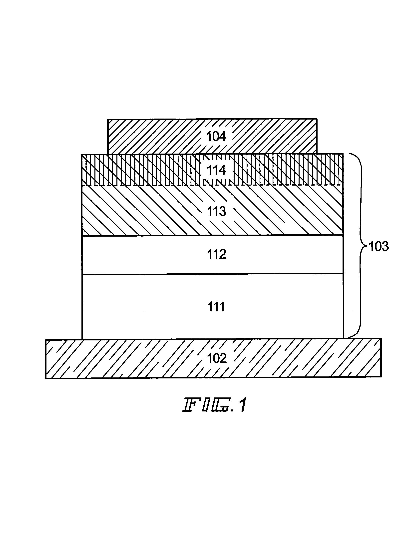
[0050]The element structure of a light emitting device of the present invention is explained using FIG. 1.

[0051]An organic compound layer 103 is formed on an anode 102 in FIG. 1, and a cathode 104 is formed on the organic compound layer 103. Note that holes are injected to the organic compound layer 103 from the anode 102, and electrons are injected to the organic compound layer 103 form the cathode 104. The holes and the electrons recombine in the organic compound layer 103, and thus luminescence is obtained.

[0052]Further, the organic compound layer 103 contains at least a hole transporting layer 111, a light emitting layer 112, an electron transporting layer 113, and an electron transmitting region 114 formed in a portion of the electron transporting layer, and is formed from one layer or a plurality of layers that are laminated, having different functions with respect to carriers, such as a hole injecting layer, a hole transporting layer, or a blocking layer. N...

embodiment mode 2

[Embodiment Mode 2]

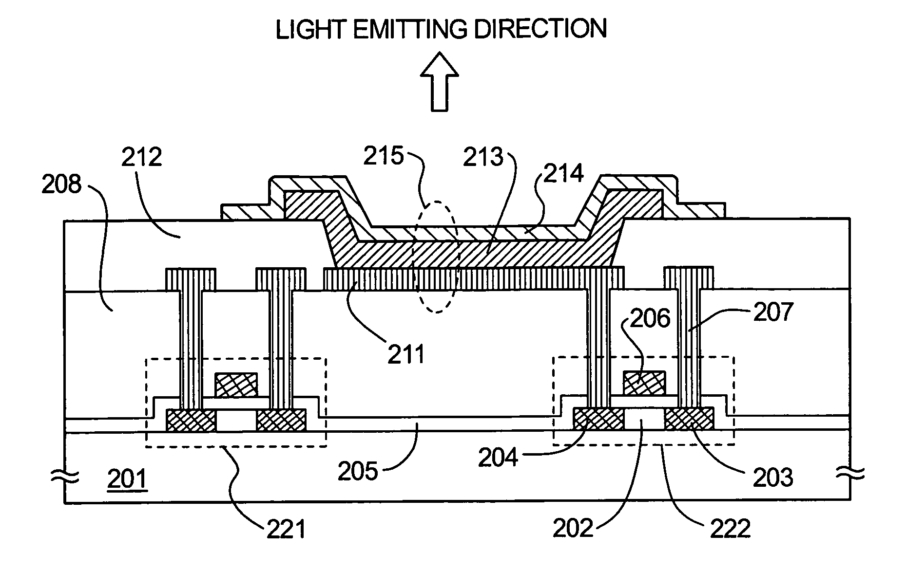
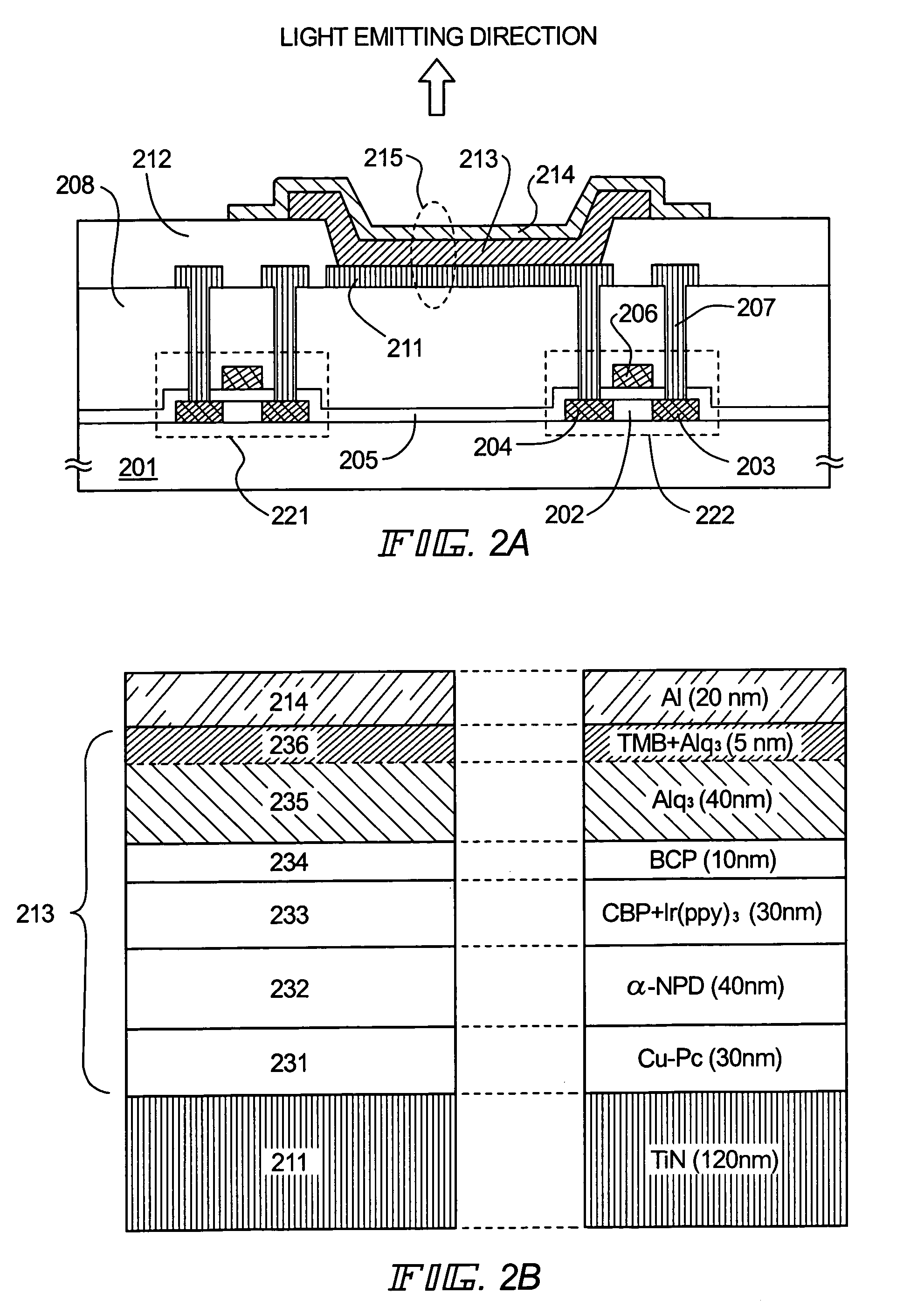
[0082]The element structure of a light emitting element in a light emitting device formed in accordance with the present invention is explained using FIGS. 2A and 2B. Note that FIG. 2A is a diagram showing the cross sectional structure of a pixel portion of a light emitting device, and FIG. 2B is a diagram showing the element structure of a light emitting element. Specifically, an upward-emission type element structure is explained for a case in which one electrode is electrically connected to an electric current control TFT, and another electrode, formed sandwiching an organic compound layer therebetween, is a cathode made from a material through which light passes.

[0083]Thin film transistors (TFTs) are formed on a substrate 201 in FIG. 2A. Note that an electric control TFT which is electrically connected to a first electrode 210 of a light emitting element 215, and which functions to control electric current supplied to the light emitting element 215, and a swit...

embodiment mode 3

[Embodiment Mode 3]

[0112]A light emitting device in which the element structure of a light emitting element differs from that of the light emitting device described in Embodiment Mode 2 is explained in Embodiment Mode 3 using FIGS. 4A and 4B. FIG. 4A is a diagram showing the cross sectional structure of a pixel portion of the light emitting device, and FIG. 4B is a diagram showing the element structure of the light emitting element. Specifically, an upward-emission type element structure is explained for a case in which one electrode is electrically connected to an electric current control TFT, and another electrode, formed sandwiching an organic compound layer therebetween, is an anode made from a material through which light passes.

[0113]Note that the light emitting device in Embodiment Mode 3 has an electric current control TFT 422 and a switching TFT 421 on a substrate 401, similar to that of Embodiment Mode 2, and it is preferable that the electric current control TFT 422 be fo...


PUM

PropertyMeasurementUnit
thicknessaaaaaaaaaa
thicknessaaaaaaaaaa
thicknessaaaaaaaaaa

Abstract

By doping an organic compound functioning as an electron donor (hereinafter referred to as donor molecules) into an organic compound layer contacting a cathode, donor levels can be formed between respective LUMO (lowest unoccupied molecular orbital) levels between the cathode and the organic compound layer, and therefore electrons can be injected from the cathode, and transmission of the injected electrons can be performed with good efficiency. Further, there are no problems such as excessive energy loss, deterioration of the organic compound layer itself, and the like accompanying electron movement, and therefore an increase in the electron injecting characteristics and a decrease in the driver voltage can both be achieved without depending on the work function of the cathode material.

Description

BACKGROUND OF THE INVENTION[0001]1. Field of the Invention[0002]The present invention relates to a light emitting device and a manufacturing method thereof using a light emitting element which has a film containing an organic compound (hereinafter referred to as an “organic compound layer”) between a pair of electrodes and which can give fluorescence or luminescence by receiving an electric field. The light emitting device referred to in the present specification is an image display device, a light emitting device or a light source. Additionally, the following are included in examples of the light emitting device: a module wherein a connector, for example, a flexible printed circuit (FPC) or a tape automated bonding (TAB) tape, or a tape carrier package (TCP) is set up onto a light emitting element; a module wherein a printed wiring board is set to the tip of a TAB tape or a TCP; and a module wherein integrated circuits (IC) are directly mounted on a light emitting element in a chip...

Claims


Application Information

Patent Timeline
Patent Type & Authority Patents(United States)
IPC IPC(8): H01L35/24H01L33/00H01L27/32H01L51/00H01L51/30H01L51/50H01L51/52
CPCH01L51/0051H01L51/5048H01L51/5052H01L27/15H01L27/3244H01L27/3295H01L51/002H01L51/0034H01L51/0035H01L51/0036H01L51/0037H01L51/0041H01L51/0059H01L51/0062H01L51/0064H01L51/0078H01L51/0081H01L51/0084H01L51/0085H01L51/5036H01L51/5206H01L2251/5315H10K59/122H10K59/173H10K59/12H10K71/30H10K85/10H10K85/143H10K85/111H10K85/1135H10K85/611H10K85/113H10K85/649H10K85/652H10K85/631H10K85/311H10K85/341H10K85/324H10K85/342H10K50/125H10K50/155H10K50/165H10K50/16H10K50/15H10K50/81H10K2102/3026H10K50/14
Inventor NISHI, TAKESHISEO, SATOSHI
Owner SEMICON ENERGY LAB CO LTD
Why Eureka
Try Eureka